
High-Performance 12-Layer ENIG + Плата с золотым пальцем Обзор продукта
The 12-Layer Gold Finger PCB is a hallmark product in the high-end печатная плата промышленность, engineered specifically for electronic equipment demanding extreme reliability, stable electrical connections, and frequent plugging/unplugging cycles. UGPCB employs advanced manufacturing processes and premium materials (ФР-4 ТГ170), combining 2м” Химическое никель, иммерсионное золото (СОГЛАШАТЬСЯ) surface finish with 30м” Hard Gold Finger Plating технология. We deliver a comprehensive high-reliability PCB solution for applications ranging from industrial controls to advanced communication systems.

Определение продукта
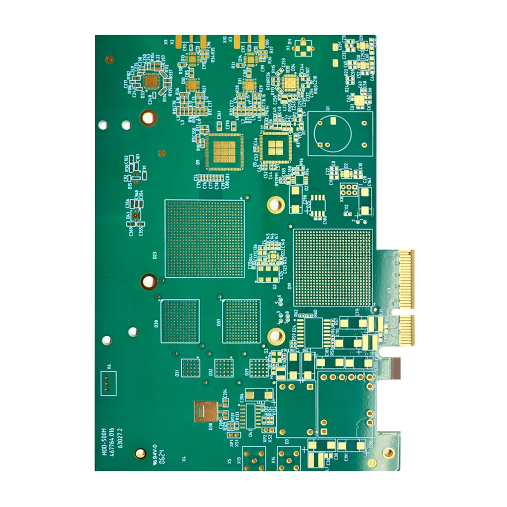
A Gold Finger PCB refers to a circuit board featuring a series of exposed, rectangular contact pads plated with thick gold (“fingers”) along one edge. These boards are designed for direct insertion into a matching connector slot, establishing a stable, pluggable connection for electrical signals and power between devices. This product is a 12-layer multilayer PCB with a standard thickness of 1.60мм, offering an optimal balance between complex circuit integration and mechanical robustness.
Критические соображения дизайна
-
Gold Finger Area Design:
-
Chamfer (Bevel) Edge (Typically 20-45°): Facilitates smooth insertion into the connector—a critical aspect of Золотой палец дизайн печатной платы.
-
Lead-in (Trace Fanout): Connections from the gold fingers to internal traces must have smooth curves, avoiding right angles to prevent stress concentration and plating cracks.
-
Solder Mask Clearance (Solder Mask Define): The gold finger area requires precise solder mask opening to ensure a clean, exposed plating surface.
-
-
Контроль импеданса & Целостность сигнала: Как 12-layer precision PCB, strict impedance control (например, 50Ом несимметричный, 100Ом дифференциал) for high-speed signal layers is essential. Stack-up design must be optimized via simulation to minimize crosstalk.
-
Thermal & Reliability Management: High-Tg material, coupled with a well-designed via structure, ensures the high-layer-count PCB operates stably in elevated temperature environments. Нанесенные сквозными отверстиями (ПТХ) should be avoided at the root of gold fingers to prevent fluid entrapment and structural weakness.
Как это работает & Структура
This PCB facilitates complex circuit interconnections through its internal 12 conductive layers. The core functionality resides in the Hard Gold Plated Fingers. The durable 30-microinch gold plating provides excellent conductivity, стойкость к окислению, and wear resistance. When the board is inserted into a backplane or card-edge connector, the gold fingers make tight, low-resistance electrical contact with the connector’s spring contacts, transmitting signals and power. The board core uses ФР-4 ТГ170, providing solid mechanical support and electrical insulation.
Основные материалы & Технические характеристики
-
Базовый материал: ФР-4 ТГ170. A high-performance epoxy glass laminate.
-
Высокая температура перехода стекла (Тс ≥ 170°С): Significantly enhances the PCB’s mechanical stability and heat resistance under high-temperature operating conditions, preventing delamination and Z-axis expansion.
-
Superior Electrical Properties: Низкая диэлектрическая проницаемость (Дк) и коэффициент рассеивания (Дф), suitable for mid-to-high frequency applications.
-
High Mechanical Strength: Ensures the 1.6mm thick PCB board resists bending and warping in mating/unmating and high-vibration environments.
-
-
Поверхностная отделка:
-
Board Surface: Химическое никель, иммерсионное золото (СОГЛАШАТЬСЯ, 2м”): Предоставляет квартиру, coplanar surface for reliable soldering of fine-pitch components and offers excellent oxidation resistance.
-
Золотые пальцы: Selective Electroplated Hard Gold (30м”): High hardness, superior abrasion resistance, and extended mating cycle life, capable of withstanding 500+ insertion/withdrawal cycles with ease.
-
Ключевые особенности & Преимущества
-
Unmatched Reliability: FR-4 TG170 high-Tg material и 12-layer precision lamination ensure long-term stability in harsh operating conditions.
-
Extended Mating Cycle Life: 30м” thick hard gold fingers far exceed standard plating thickness, offering exceptional wear resistance—the ideal choice for high-durability plug-in PCBs.
-
Отличная целостность сигнала: The multilayer design provides uninterrupted reference planes for high-speed signals, and controlled impedance guarantees signal quality.
-
Robust Thermal & Механические характеристики: The 1.60mm standard thickness combined with high-Tg material delivers superior rigidity, тепловое управление, and dimensional stability.
-
Comprehensive High-End Solution: От многослойный Изготовление печатной платы к specialty surface finishing (СОГЛАШАТЬСЯ + Selective Gold), UGPCB provides full-process control, ensuring consistent, high-quality results.
Схема производственного процесса
Panelization → Inner Layer Imaging → Lamination (12-Слой) → Drilling → Desmear & Electroless Copper Deposition → Outer Layer Imaging → Pattern Plating (for Hard Gold Fingers) → Etching → Solder Mask Application → ENIG Surface Finish → Gold Finger Beveling → Electrical Test (Летающий зонд / Fixture) → Final Automated Optical Inspection (АОИ) → Packaging.
Основные приложения & Варианты использования
This product is the core component of high-end electronic devices requiring direct board-to-board plug connections или integration into backplane systems.
-
Промышленные системы управления: PLC modules, industrial computer motherboards, servo drives, I/O interface cards.
-
Телекоммуникации & Networking Equipment: Router/switch line cards, optical transceiver modules, baseband processing units.
-
Медицинская электроника: Data acquisition and processing boards for advanced medical imaging systems (например, КТ -сканеры, ultrasound machines).
-
Тест & Измерительные приборы: Plug-in modules for high-end oscilloscopes, анализаторы спектра, and Automated Test Equipment (ЕЛ).
-
Аэрокосмическая промышленность & Defense Electronics: Mission-critical avionics systems and radar signal processing modules where reliability is paramount.

Классификация научной продукции
-
По количеству слоев: High-Layer-Count / Многослойная плата (≥8 layers, конкретно 12 слои).
-
By Special Feature/Process: Золотой палец (Gold Edge Connector) печатная плата, Mixed Surface Finish PCB (СОГЛАШАТЬСЯ + Selective Hard Gold).
-
By Material Property: Высокий Тг (TG170) печатная плата, FR-4 Series PCB.
-
By Application Grade: Industrial-Grade PCB, Telecom-Grade PCB, High-Reliability PCB.
Why Choose UGPCB’s 12-Layer Gold Finger PCB?
We understand that a reliable Gold Finger PCB is the foundation of your high-end equipment’s stable operation. Использование глубокого опыта в многослойный Производство печатных плат и specialty surface finish processes, UGPCB guarantees that every board delivered meets military-grade reliability standards with commercial-grade delivery efficiency. We provide not just a product, but a customized PCB solution.
Contact our technical sales team today to discuss your project requirements, receive a detailed quote, and qualify for a free design-for-manufacturability (DFM) обзор and sample program. Partner with UGPCB for your most demanding 12 слой печатной платы приложения.


