

Обзор печатной платы P2.9
P2.9 светодиодная печатная плата (печатная плата) является специализированным печатная плата предназначен для использования со светодиодными модулями P2.9, которые обычно используются в приложениях дисплея с высоким разрешением. Эта печатная плата идеально подходит для создания больших, Бесплатные светодиодные дисплеи.
Что такое съемная плата с светодиодной печатной платой P2.9?
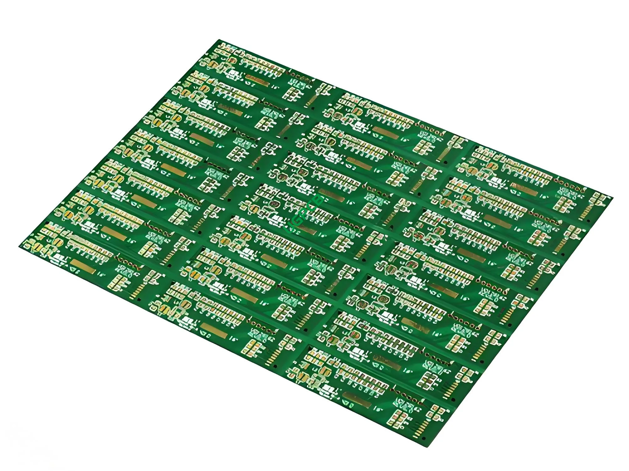
Печатная плата светодиода P2.9 представляет собой печатная плата (печатная плата) Специально разработано для размещения и подключения светодиодных модулей P2.9. Термин “P2.9” относится к пиксельному шагу светодиодного модуля, который измеряет 2.9 миллиметры между каждым пикселем. Эта печатная плата гарантирует, что светодиодные модули могут быть эффективно взаимосвязаны, Предоставление стабильной платформы для электронных компонентов.
Требования к дизайну
Требования к проектированию для печатной платы с светодиодной печатной платой P2.9 строгими для обеспечения ее производительности и надежности:
- Материал: SY1000-2 TG170 FR4, выбрано для его превосходных электрических и тепловых свойств.
- Количество слоев: 6 слои для размещения необходимой схемы и целостности сигнала.
- Цвет: Черный/белый для легкой идентификации и эстетической привлекательности.
- Готовая толщина: 1.0мм для обеспечения структурной целостности и долговечности.
- Толщина меди: 1Оз для обеспечения адекватной проводимости и рассеяния тепла.
- Обработка поверхности: Погружение золота для повышения припая и коррозионной устойчивости.
- Минимальная трассировка и пространство: 4мил(0.1мм) для поддержки тонких схем схемы.
- Характеристика: Больше прокладки с небольшим интервалом для размещения плотной планировки светодиодных модулей P2.9.
Как это работает?
Светодиодная печатная плата P2.9 работает, предоставляя платформу для различных электронных компонентов, которые должны быть взаимосвязаны через проводящие пути. Эти пути, или следы, изготовлены из меди и запечатлены на доске. Материал SY1000-2 TG170 FR4 гарантирует, что печатная плата может противостоять требованиям приложений светодиодного отображения, В то время как обработка поверхности погружения в погружение гарантирует, что эти следы остаются проводящими и устойчивыми к коррозии.
Приложения
Основное применение платы с светодиодной печатной платой P2.9 находится в светодиодных системах с высоким разрешением, где управляет и регулирует поток электрических сигналов.. Это включает в себя:
- Внутренние и открытые светодиодные дисплеи
- Цифровые вывески
- Видеостры большого формата
- Стадии мероприятия и концертные экраны
Классификация
На основе его функций и приложений, Плата с помощью светодиодной печатной платы P2.9 может быть классифицирована как высокая плотность, Высокоскоростная цифровая печатная плата предназначен для светодиодных дисплеев. Эта классификация подчеркивает его способность обрабатывать высокочастотные сигналы и обеспечивать стабильные электрические соединения.
Материальная композиция
Ядро материал В печатной плате светодиодов P2.9 используется SY1000-2 TG170 FR4., высокопроизводительный композитный материал, известный своим превосходным механическим, тепло, и электрические свойства. Этот материал гарантирует, что печатная плата может противостоять требованиям приложений светодиодного отображения.
Характеристики производительности
Характеристики производительности платы с светодиодной печатной платой P2.9 включают:
- Высокая целостность сигнала
- Низкая потеря сигнала
- Превосходное тепловое управление
- Надежная механическая прочность
- Долгосрочная стабильность
Структурные детали
Структурные детали платы с светодиодной печатной платой P2.9 заключаются в следующем:
- Количество слоев: 6 слои
- Готовая толщина: 1.0мм
- Толщина меди: 1ОЗ
- Обработка поверхности: Погружение Золото
- Минимальная трассировка и пространство: 4мил(0.1мм)
- Характеристика: Больше прокладки с небольшим интервалом для размещения плотной планировки светодиодных модулей P2.9.
Функции и преимущества
Ключевые функции и преимущества печатной платы P2.9 включают:
- Взаимодействие высокой плотности
- Отличная целостность сигнала
- Надежная механическая конструкция
- Надежная долгосрочная производительность
- Эстетические варианты цвета (Черный/белый)
Производственный процесс
Производственный процесс печатной платы P2.9 включает в себя несколько этапов, включая:
- Выбор материала: Выбор высококачественного материала SY1000-2 TG170 FR4.
- Наложение слоев: Аранжировка 6 слои с точностью.
- Офорт: Удаление лишней меди, чтобы сформировать желаемые схемы трассировки.
- Прикладная маска: Применение слоя припоя маски для защиты медных следствий.
- Покрытие: Применение обработки поверхности погружения в погружение.
- Сборка: Включение PTH и VIAS для взаимосвязей слоя.
- Тестирование: Обеспечение печатной платы соответствует всем спецификациям производительности.
Варианты использования
Плата с светодиодной печатной платой P2.9 используется в различных сценариях, таких как:
- Внутренние и наружные светодиодные дисплеи с высоким разрешением
- Цифровые установки вывесок
- Стадии концерта и событий с большими видеоилками
- Розничные среды с динамичными рекламными экранами


