
In the era of exploding data center traffic and widespread 5G deployment, traditionell PCB -Materialien can no longer support 25Gbps or 112Gbps high-speed signal transmission. When Signal Integrity (UND) and Power Integrity (PI) become major design hurdles, a high-performance 20-Schicht Hochgeschwindigkeitsplatine emerges as the essential tool for hardware engineers.
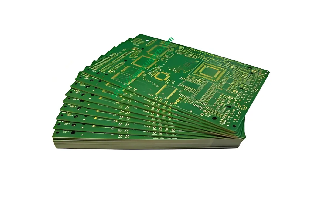
UGPCB utilizes advanced manufacturing and strict material control to offer the 20-layer high-speed PCB (Communication Backplane) . Featuring high-end TUC/TU872LK material, combined with blind via and hard gold technology, it provides exceptional physical support for servers, core routers, and aerospace equipment. This article details the technical features and core value of this product.
1. Produktübersicht: What is a 20-Layer High-Speed PCB?
A PCB is the foundation of electronic products . As systems demand higher speeds and densities, standard 2-layer or 4-layer boards struggle with impedance control and EMI shielding.
UGPCB 20-layer high-speed PCB consists of 20 conductive copper layers laminated with Prepreg and Core . Designed specifically as a communication backplane, it manages data transmission and power distribution between line cards. This is a high-end solution for low-loss transmission and complex system integration.
2. Design & Material: The Superiority of TU872LK
A high-quality mehrschichtige Leiterplatte relies on both intelligent design and premium materials. UGPCB adheres to strict high-speed design rules:
-
Stackup Design: The 20-layer structure ensures tight coupling between signal and ground planes. Critical high-speed signals are embedded as striplines for optimal EMC performance . Multiple ground planes effectively reduce PDN impedance .
-
Material Selection—TUC/TU872LK:
For signals above 10Gbps, standard FR-4 suffers from high dielectric loss. UGPCB selects TU-872LK, a high-performance modified epoxy from TUC, Ideal für Hochgeschwindigkeitsdesigns .-
Niedriger Verlust: Its Dissipation Factor (Df) is extremely low (< 0.009 bei 10 GHz), ensuring signal integrity across complex 20-layer paths .
-
Hohe thermische Zuverlässigkeit: With a Tg of 220°C (DMA), it guarantees dimensional stability and CAF resistance during lamination and operation .
-
3. Struktur & Arbeitsprinzip
Das blind and buried via PCB operates on transmission line theory. High-speed signals use adjacent reference layers (GND) for a clear return path, creating uniform impedance.
-
Structural Feature:
-
Blind Via Technology: The design includes L3-L20 blind vias . These vias start at layer 3 and stop at layer 20, saving routing space and reducing signal-reflecting stubs—a key process for high-speed interconnects on communication backplane PCBs .
-
-
Physical Specifications:
-
Fertige Dicke: The 5.0mm thickness and 1OZ copper provide the mechanical strength needed to support heavy connectors during backplane insertion .
-
4. Core Performance and Precision Manufacturing
UGPCB demonstrates advanced capabilities with this 20-layer hard gold circuit board:
-
Fine Line Capability: Minimum line width/space is 4mil/4mil . Achieving this on a 5.0mm thick board is a challenge that UGPCB meets with LDI technology.
-
Surface Finish—Hard Gold: Utilizing a Hard Gold 3-15U process .
-
Unlike soft gold, hard gold includes elements like cobalt for higher wear resistance.
-
Dies ist von entscheidender Bedeutung für communication PCBs. Backplanes connect via gold fingers that endure frequent insertion cycles. Hard gold ensures long-term contact reliability.
-
-
Prozessfluss:
Material Prep (TU872LK) → Inner Layer Imaging (4Mil) → AOI → Layup (20-Layer Lamination) → Bohren (L3-L20 Blind Vias) → Plating → Outer Layer Imaging → Hard Gold → Solder Mask → Profiling → Testing.
5. Classification and Applications
This product fits precise industry classifications:
-
Für Schichtzahl: 20-Layer Multilayer PCB
-
Durch Material: High-Speed Digital PCB (Low Loss Material)
-
Nach Prozess: Blind & Buried Via Board
-
Durch Anwendung: Communication Backplane PCB / System Motherboard
Typische Anwendungen:
-
Core Switches & Router: Acts as a chassis backplane handling 400G/800G data traffic.
-
5G Basisstationen: Supports high-speed interconnects in Baseband Units.
-
Hochleistungs-Computing (HPC): Ensures signal integrity for PCIe channels in servers.

6. Warum wählen Sie UGPCB??
Manufacturing a 20-layer high-speed PCB tests material properties, lamination alignment, and drilling accuracy.
-
Precision Impedance Control: Leveraging TU872LK’s Dk/Df properties, we control impedance tolerance to within ±5% .
-
Hard Gold Process: Our controlled plating ensures uniform gold thickness (3-15U) and a corrosion-resistant nickel layer, supporting thousands of insertion cycles.
-
Full Traceability: Every board meets communication-grade standards, verified through strict quality checks from material to delivery.
Get a Quote Today
If you are seeking a reliable partner for high-layer, high-speed backplanes capable of handling 112G/224G SerDes signals, UGPCB is your trusted choice.
[Kontaktieren Sie uns] for a quote.


