
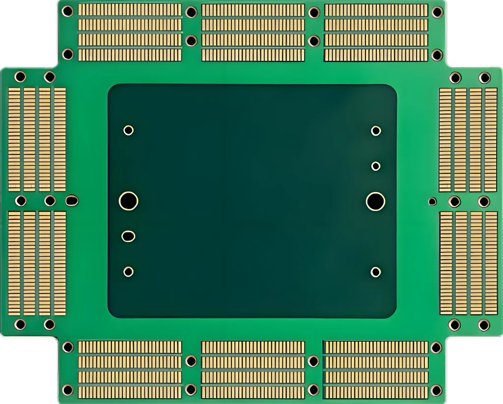
Einführung in die 58-Schicht Atzladung PCB
Die 58-Schicht aß (Automatisierte Testausrüstung) Lastplatine ist eine hohe Dichte, Mehrschicht Leiterplatte entwickelt für Präzisionssignalübertragung und Haltbarkeit in anspruchsvollen Testumgebungen. Mit fortschrittlichen Parametern entworfen, Es gewährleistet eine optimale Leistung bei hochfrequenten und leistungsstarken Anwendungen.
Schlüsselspezifikationen
-
Schichten: 58
-
Abmessungen: 17.2″ x 17,8″
-
Dicke: 230 Mil
-
Material: FR4 TG185
-
Mindestlochgröße: 5 Mil
-
BGA -Abstand: 0.8 mm
-
Seitenverhältnis: 23.4:1
-
Drill-to-Kupfer-Distanz: 7 Mil
-
POFV (Überfüllt überfüllt über): Ja
-
Rückenbohrungen: NEIN
-
Oberflächenbeschaffung: ENEG+TG+nur
Design- und strukturelle Merkmale
Überlegungen zum kritischen Design
-
Hohe Schichtzahl: Die 58-Schicht-Struktur unterstützt das komplexe Routing für Verbindungen mit hoher Dichte (HDI), Minimierung des Signalverlusts.
-
Materialauswahl: FR4 TG185 sorgt für die thermische Stabilität (bis zu 185 ° C Glasübergangstemperatur), kritisch für Hochleistungsanwendungen.
-
Präzisionsbohrungen: A 5 mil Mindestlochgröße und 23.4:1 Das Seitenverhältnis ermöglicht eine zuverlässige Mikrovia -Bildung, Wesentlich für BGA (0.8 MM -Tonhöhe) Komponentenintegration.
-
Signalintegrität: Kontrollierte Impedanz und 7 MIL-Drill-to-Kupfer-Abstand reduzieren das Übersprechen und elektromagnetische Störungen (EMI).
Einzigartige strukturelle Vorteile
-
POFV -Technologie: Verbessert durch Zuverlässigkeit durch Füllen und Plattieren von Vias, Verbesserung der thermischen und mechanischen Leistung.
-
ENEG+TG+REIG -Oberflächenfinish: Kombiniert elektrololes Nickel elektrololes Gold (Eneg) und eintauchen Gold (ZUSTIMMEN) für überlegene Korrosionsbeständigkeit und Lötlichkeit.
Leistung und Anwendungen
Betriebliche Prinzipien
Die PCB erleichtert eine präzise elektrische Signalrouting über 58 Schichten, Nutzung der dielektrischen Eigenschaften von FR4 TG185, um die Signalintegrität aufrechtzuerhalten. POFV sorgt für robuste Verbindungen in Hochstressumgebungen, Während das optimierte Seitenverhältnis stabile Hochfrequenzoperationen unterstützt.
Wichtige Leistungsmetriken
-
Thermischer Widerstand: Stand den Temperaturen bis zu 185 ° C.
-
Mechanische Stabilität: Hoch -TG -Material verhindert die Delaminierung unter thermischem Radfahren.
-
Signalgeschwindigkeit: Dielektrisches Material mit niedrigem Verlust minimiert die Latenz.
Primäre Anwendungsfälle
-
Automatisierte Testausrüstung (ASS): Verwendet in Halbleiter -Testsystemen zur Validierung von ICs und Mikroprozessoren.
-
Luft- und Raumfahrt und Verteidigung: Eingesetzt in Radar- und Kommunikationssystemen, die eine hohe Zuverlässigkeit erfordern.
-
Telekommunikation: Unterstützt 5G-Infrastruktur und Hochgeschwindigkeitsdatenübertragung.
-
Kfz -Elektronik: In ADAS integriert (Fortgeschrittene Fahrerhilfesysteme) und EV -Leistungsmodule.
Produktionsprozess und Qualitätssicherung
Fertigungsworkflow
-
Materialvorbereitung: FR4 TG185 Laminate werden auf 17,2 geschnitten″ x 17,8″ Abmessungen.
-
Laserbohren: Schafft 5 Mil microvias mit a 23.4:1 Seitenverhältnis.
-
Beschichtung und Füllung: Die POFV -Technologie wendet die Kupferbeschichtung auf gefüllte Vias an.
-
Layer -Stackup: 58 Schichten sind ausgerichtet und unter hohem Druck gebunden.
-
Oberflächenbearbeitung: ENEG+TG+Enig -Beschichtung wird zum Korrosionsschutz angewendet.
-
Testen: Elektrische Kontinuität, Impedanz, und thermische Spannungstests werden durchgeführt.
Qualitätskontrollstandards
-
IPC-6012 Klasse 3: Gewährleistet die Zuverlässigkeit für harte Umgebungen.
-
Impedanzkontrolle: ± 10% Toleranz beibehalten.
Zusammenfassung der Vorteile
-
Hochdichte Design: Unterstützt komplexe Schaltkreise in kompakten Räumen.
-
Thermische Widerstandsfähigkeit: FR4 TG185 sorgt für die Stabilität unter extremen Bedingungen.
-
Präzisionstechnik: 5 MIL -Löcher und 0,8 mm BGA -Abstand ermöglichen die Integration der miniaturisierten Komponenten.
-
Vielseitige Anwendungen: Von Semiconductor -Tests bis zur 5G -Infrastruktur.
Diese PCB kombiniert modernes Design, strenge Fertigungsstandards, und robuste Materialien, um den Bedürfnissen der missionskritischen Industrie zu erfüllen.


