

Materialzusammensetzung
Das Aluminium-Nitrid-Keramikplatik besteht aus hochwertigen Keramikmaterialien, Speziell Keramik -PCB und Keramiksubstrat. Diese Kombination sorgt für eine außergewöhnliche thermische Leitfähigkeit und elektrische Isolationseigenschaften.
Leistungseigenschaften
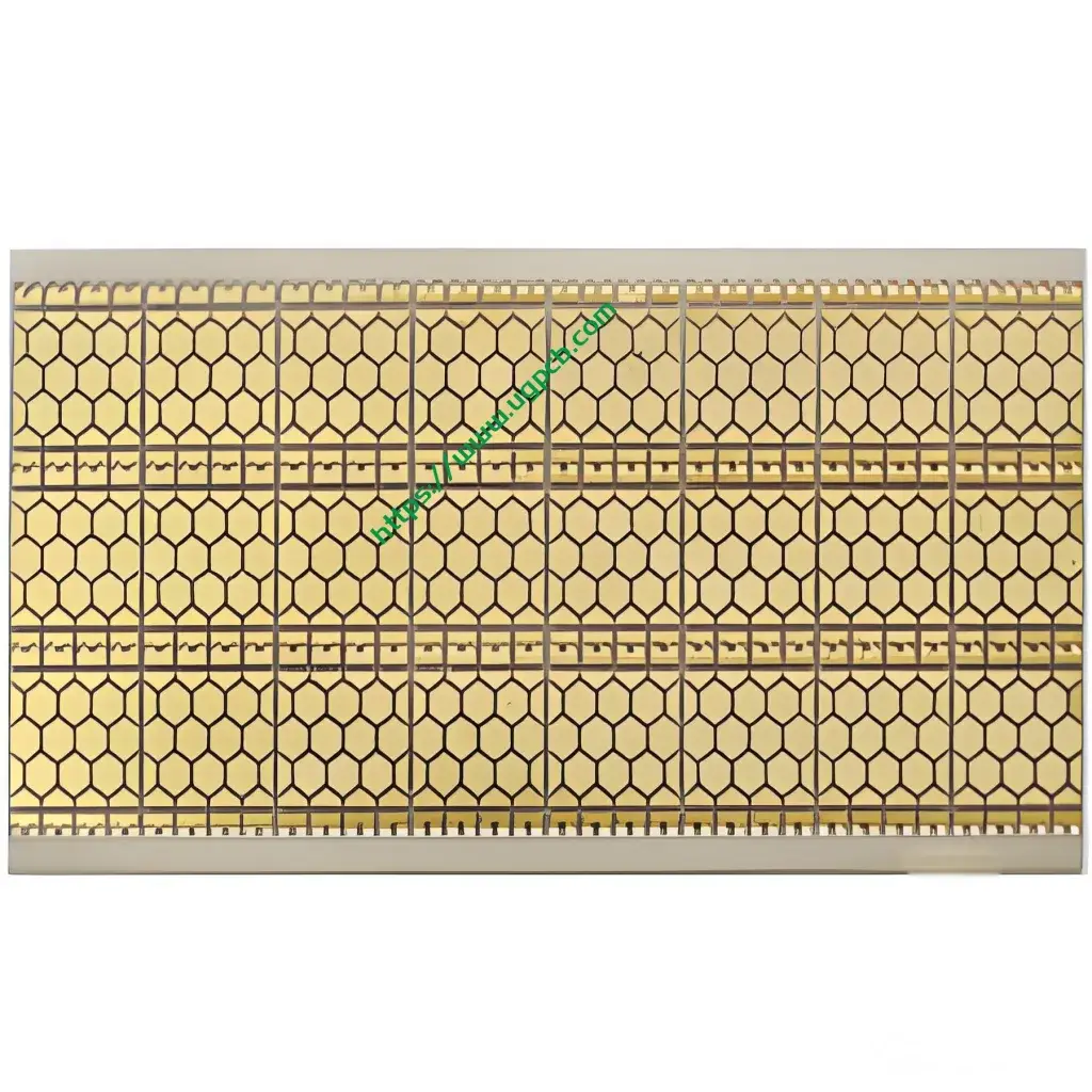
Der Leiterplatte features a 2-layer ceramic structure with a white color appearance. Die Dicke der Aluminiumnitridschicht beträgt genau 0,635 mm, providing a sturdy base for Komponenten. Die Kupferdicke von 1 Unzen (35eins) sorgt für eine gute elektrische Leitfähigkeit, während die Eintauchdicke mit einer Golddicke von >= 3U” Verbessert die Korrosionsbeständigkeit und sorgt für reibungslose Lötprozesse.
Unterscheidungsmerkmale
- Hohe thermische Leitfähigkeit: Aluminiumnitrid bietet eine hervorragende thermische Leitfähigkeit, Damit für Hochleistungs- und Hochfrequenzanwendungen geeignet ist.
- Haltbarkeit: Keramikmaterialien sind bekannt für ihre Härte und Haltbarkeit, Beitrag zur langen Lebensdauer der PCB.
- Präzision: Die minimale Blende von 0,8 mm ermöglicht die Platzierung feiner Komponenten, Gewährleistung von Verpackungen mit hoher Dichte.
Produktionsprozess

Die Produktion von Aluminiumnitrid -Keramik -PCBs umfasst mehrere kritische Schritte:
- Materialvorbereitung: Hochwertige Aluminiumnitridpulver und andere Keramikmaterialien werden gemischt und in die gewünschte Form gedrückt.
- Sintern: Das gepresste Keramik -Substrat unterzieht sich bei hohen Temperaturen, um die erforderliche Dichte und Stärke zu erreichen.
- Kupferablagerung: Eine Kupferschicht wird am Keramiksubstrat unter Verwendung erweiterter Metallisationstechniken abgelagert.
- Schaltungsstrukturierung: Die Kupferschicht ist geätzt, um die gewünschten Schaltungsmuster zu bilden.
- Lochbohrung: Durch Löcher werden gebohrt, um Verbindungen zwischen Schichten zu ermöglichen.
- Keramikdammtechnologie: Diese einzigartige Technologie sorgt für die genaue Ausrichtung und Versiegelung von Löchern, Verbesserung der Zuverlässigkeit der PCB.
- Oberflächenbehandlung: Die Leiterplatte unterliegt ein, um eine korrosionsbeständige Oberfläche zu ermöglichen, um eine Goldbeschichtung zu erhalten.
Anwendungsszenarien
Aluminium-Nitrid-Keramik-PCBs sind ideal für verschiedene Hochleistungsanwendungen:
- Hochleistungselektronik: Geeignet für den Einsatz in Netzteilen, Wechselrichter, und andere elektronische Hochleistungsgeräte aufgrund ihrer hervorragenden thermischen Verwaltungsfähigkeiten.
- Hochfrequenzkreise: Perfekt für HF- und Mikrowellenschaltungen, die einen geringen Verlust und eine hohe Stabilität erfordern.
- Medizinische Ausrüstung: Wird in medizinischen Geräten verwendet, die Präzision erfordern, Zuverlässigkeit, und Hochleistungselektronik.
- Luft- und Raumfahrt und Verteidigung: Ideal für Anwendungen in harten Umgebungen, in denen Haltbarkeit und thermischer Widerstand von entscheidender Bedeutung sind.
Zusammenfassend, Aluminium -Nitrid -Keramik -PCBs bieten eine Kombination aus außergewöhnlicher thermischer Leitfähigkeit, Haltbarkeit, und Präzision, Sie ideal für Hochleistungselektronik in verschiedenen Branchen ideal machen.


