
UGPCB Standard 2-lagige starre Leiterplatte: Zuverlässige 1,6-mm-FR-4-Leiterplatten für anspruchsvolle Anwendungen
Das Herzstück moderner Elektronik, Die Leiterplatte (Leiterplatte) fungiert als grundlegende Plattform, Komponenten miteinander verbinden und Signale präzise weiterleiten. UGPCB Standardmäßige 2-lagige starre Leiterplatte, gebaut mit einem robusten 1.60mm Dicke und leistungsstark FR-4 TG150-Material, stellt die optimale Balance der Haltbarkeit dar, elektrische Leistung, und Wirtschaftlichkeit für ein breites Anwendungsspektrum. Das doppelseitige Leiterplatte ist eine bewährte Lösung für Prototypen und elektronische Geräte mittlerer Komplexität.
Produktdefinition & Einstufung
Technische Klassifizierung:
-
Für Schichtzahl: Doppelseitige Leiterplatte / Zweischichtige Leiterplatte
-
Durch die Steifigkeit des Substrats: Starre PCB
-
Nach Basismaterial: Glasepoxidharz (FR-4) Leiterplatte
-
Nach Brennbarkeitsbewertung: UL94 V-0 (FR-4 inhärent)
-
Durch Montagekompatibilität: Durchloch-Technologie (Tht) und Oberflächenmontagetechnologie (SMT) leistungsfähige Leiterplatte.
Bei diesem Produkt handelt es sich um ein doppelseitige Leiterplatte Hergestellt aus kupferkaschiertem Laminat auf beiden Seiten eines isolierenden FR-4-Kerns. Die elektrische Verbindung zwischen den Schichten wird über plattierte Durchgangslöcher erreicht (PTH). Der 1.60mm (etwa 1/16 Zoll) Brettdicke ist ein Industriestandard, bietet eine hervorragende mechanische Stabilität.
Konstruktion & Materialspezifikationen
Schichtaufbau:
Das 2 Schicht starre PCB Die Struktur ist wie folgt (von oben nach unten):
-
Obere Lötmaske (Weiß): Isolierschicht zur Vermeidung von Lötbrücken.
-
Obere Kupferschicht (1 oz, ~35µm): Geätzt, um Leiterbahnen und Pads zu bilden.
-
Isolierendes Kernsubstrat (FR-4, Tg150): Bietet mechanische Unterstützung und elektrische Isolierung.
-
Untere Kupferschicht (1 oz, ~35µm): Geätzt, um Schaltkreise auf der unteren Schicht zu bilden.
-
Untere Lötmaske (Weiß): Isolierende Schutzschicht.
-
Siebdruck-Legende (Schwarz): Komponentenbezeichner, Logos, und Markierungen.
Schlüsselmaterialien:
-
Basislaminat: FR-4 TG150. Dies bezeichnet ein flammhemmendes glasfaserverstärktes Epoxidlaminat mit einer Glasübergangstemperatur (Tg) von 150°C. Es bietet eine hervorragende mechanische Festigkeit, elektrische Isolierung, und thermische Zuverlässigkeit für a starre Leiterplatte, Damit ist es die kostengünstigste Wahl der Branche.
-
Kupferfolie: Standard 1 Unze (oz) Galvanisch abgeschiedenes Kupfer für optimale Leitfähigkeit und Stromtragfähigkeit.
-
Oberflächenbeschaffung: Bleifreie Heißluft-Lotnivellierung (Bluten). Kostengünstig und zuverlässig PCB-Oberflächenbeschaffenheit das eine hervorragende Lötbarkeit bietet, gute Haltbarkeit, und robuster Schutz vor Oxidation.
-
Tinten: Hochwertige fotobebilderbare weiße Lötstopplacktinte und langlebige schwarze Epoxid-Siebdrucktinte.
(Bildvorschlag: Querschnittsdiagramm des PCB-Aufbaus)
Alles nehmen: Detailliertes Querschnittsdiagramm von a 2 Schicht starre Leiterplatte mit Kupfer, FR-4-Kern, und Lötmaskenschichten.
Entwurfsrichtlinien & Funktionsprinzip
Überlegungen zum kritischen Design:
-
Über Design: Maximieren Sie den Routing-Platz Ihres doppelseitig PCB-Design durch die strategische Platzierung plattierter Durchgangslöcher (PTHS) für Zwischenschichtverbindungen.
-
Spurenbreite/Abstand: Für 1 Unze Kupfer, Eine standardmäßige Mindestspur/Abstand beträgt 6 mil/6 mil (~0,15mm) um eine zuverlässige Herstellbarkeit und aktuelle Kapazität sicherzustellen.
-
Unterlage & Loch-Ringring: Stellen Sie sicher, dass das Pad im Verhältnis zum Bohrloch ausreichend groß ist, um eine starke Verbindung zu gewährleisten Leiterplattenbestückung und Zuverlässigkeit.
-
Lötmaske & Siebdruck: Weiße Lötstoppmaske erleichtert die visuelle Inspektion während SMT -Baugruppe, während ein klarer schwarzer Siebdruck von entscheidender Bedeutung ist PCB -Prototyping und reparieren.
Funktionsprinzip:
Eine Leiterplatte erzeugt keine Funktion, sondern ermöglicht sie über ihre vordefinierten Leiterbahnen. Die geätzten Kupferleiterbahnen ersetzen eine diskrete Verkabelung, Bereitstellung elektrischer Verbindungen zwischen Komponenten. Das isolierende FR-4-Substrat verhindert Kurzschlüsse. Durchlöcher plattiert (PTHS) dienen als vertikale Leitungen, Ober- und Unterseite verbinden PCB-Kupferschichten, Dadurch wird die verfügbare Routingfläche im Vergleich zu einer einseitigen Platine verdoppelt und die Designflexibilität erhöht.
Leistungseigenschaften & Vorteile
-
Hohe Zuverlässigkeit: Der FR-4 TG150-Substrat sorgt für eine stabile Leistung in Umgebungen unterhalb seiner Tg, Bietet hervorragende thermische und mechanische Stabilität für a starre Leiterplatte.
-
Hervorragende elektrische Eigenschaften: Eine niedrige Dielektrizitätskonstante und ein niedriger Verlustfaktor unterstützen die Signalintegritätsanforderungen der meisten digitalen und analogen Schaltkreise.
-
Hohe Herstellbarkeit: Der 1.6mm Standardplatine Dicke Und Bleifreies HASL Prozesse sind ausgereift, Gewährleistung einer hohen Ausbeute, Kostenkontrolle, und schnelle Lieferzeiten.
-
Hervorragende Lötbarkeit: Das HASL-Finish bietet eine flache Oberfläche, Benetzbare Oberfläche, ideal für beides Durchkontaktierung Und SMT-Lötprozesse.
-
Klare Identifikation: Kontrastreiche weiße Lötmaske mit schwarzer Beschriftung erleichtert die Effizienz Leiterplatte Inspektion, Testen, und nacharbeiten.
-
Umweltkonformität: Die bleifreie HASL-Oberfläche entspricht RoHS und anderen Umweltrichtlinien.
Standard-Herstellungsprozessablauf
UGPCB hält sich durchgehend an die IPC-Standards PCB-Herstellungsprozess:
Panelisierung → Bohren → Stromlose Kupferabscheidung → Trockenfilmlaminierung & Bildgebung → Verkupferung → Ätzen → Auftragen einer Lötmaske & Aushärten → Siebdruck → Oberflächenfinish (Bleifreies HASL) → Profilierung/Routing → Elektrische Tests (Fliegende Sonde) → Abschließende automatische optische Inspektion (AOI) → Verpackung & Lieferung.
Primäranwendungen & Anwendungsfälle
Das ist vielseitig zweischichtige starre Leiterplatte wird häufig in Branchen eingesetzt, die ein Gleichgewicht zwischen Zuverlässigkeit und Wert erfordern:
-
Industriekontrollen: SPS-Schnittstellen, Sensormodule, motorische Antriebe, HMI-Controller-Boards.
-
Unterhaltungselektronik: Intelligente Gerätesteuerungen, Audioverstärker, Netzteile, pädagogische Kits.
-
Telekommunikation: Router-/Switch-Peripherieplatinen, HF-Antennenmodule, Netzwerküberwachungseinheiten.
-
Kfz -Elektronik: Infotainmentsysteme, Lichtsteuermodule, Karosseriesteuermodule (nicht sicherheitskritisch).
-
Leistungselektronik: Smart-Meter-Leiterplatten, USV-Steuerplatinen, Solar-Wechselrichter-Schaltung.
-
Prüfen & Messung: Datenerfassungskarten, Instrumentenbedienfelder, Handtesterplatinen.
Warum sollten Sie sich für UGPCB für Ihre 2-Lagen-PCB-Anforderungen entscheiden??
Wenn Sie sich für UGPCB entscheiden, müssen Sie mit einem zuverlässigen Partner zusammenarbeiten Leiterplattenhersteller der Qualität verpflichtet. Wir sind spezialisiert auf PCB-Prototyp und Produktion mittlerer Stückzahlen, Implementierung strenger elektrischer Tests und IPC-A-600-basierter Inspektionen auf jeder Platine. Von einfach 2 Schichtplatten bis hin zu komplexen mehrschichtigen Designs, Wir bieten Experten PCB-Design für die Fertigung (DFM) Support und eine optimierte Lieferkette.
Kontaktieren Sie uns noch heute für ein wettbewerbsfähiges Angebot und eine kurze Lieferzeit für Ihr 1,6-mm-FR-4-2-Lagen-PCB-Projekt!
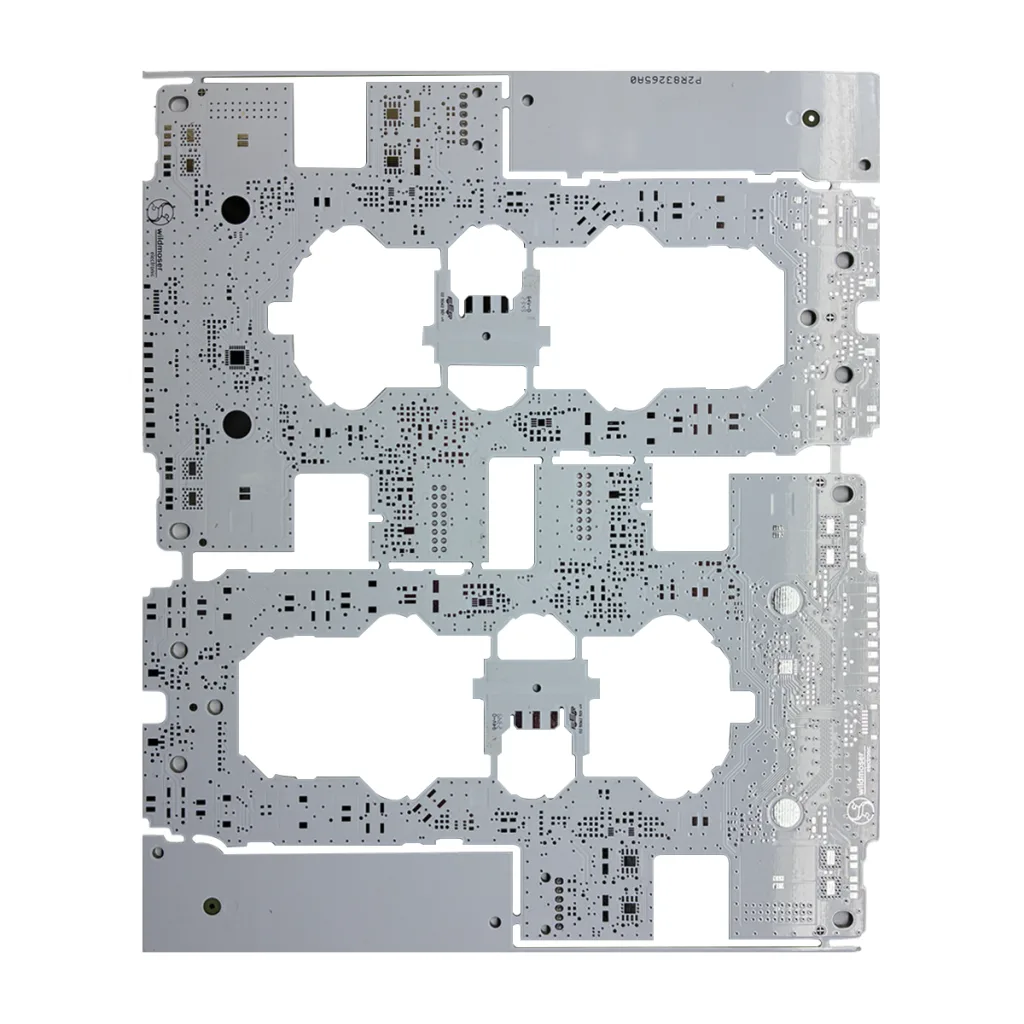
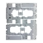
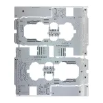
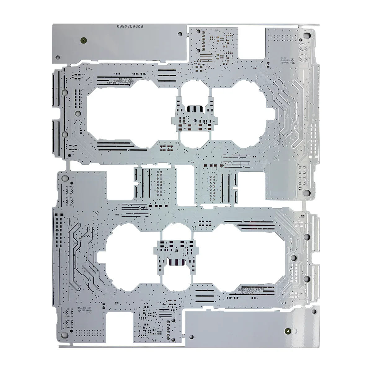
(Bildvorschlag: Galerie fertiger Leiterplatten mit unterschiedlichen Designs)
Alles nehmen: Galerie verschiedener 2 Beispiele für schichtstarre Leiterplatten, hergestellt von UGPCB, mit weißer Lötmaske.


