

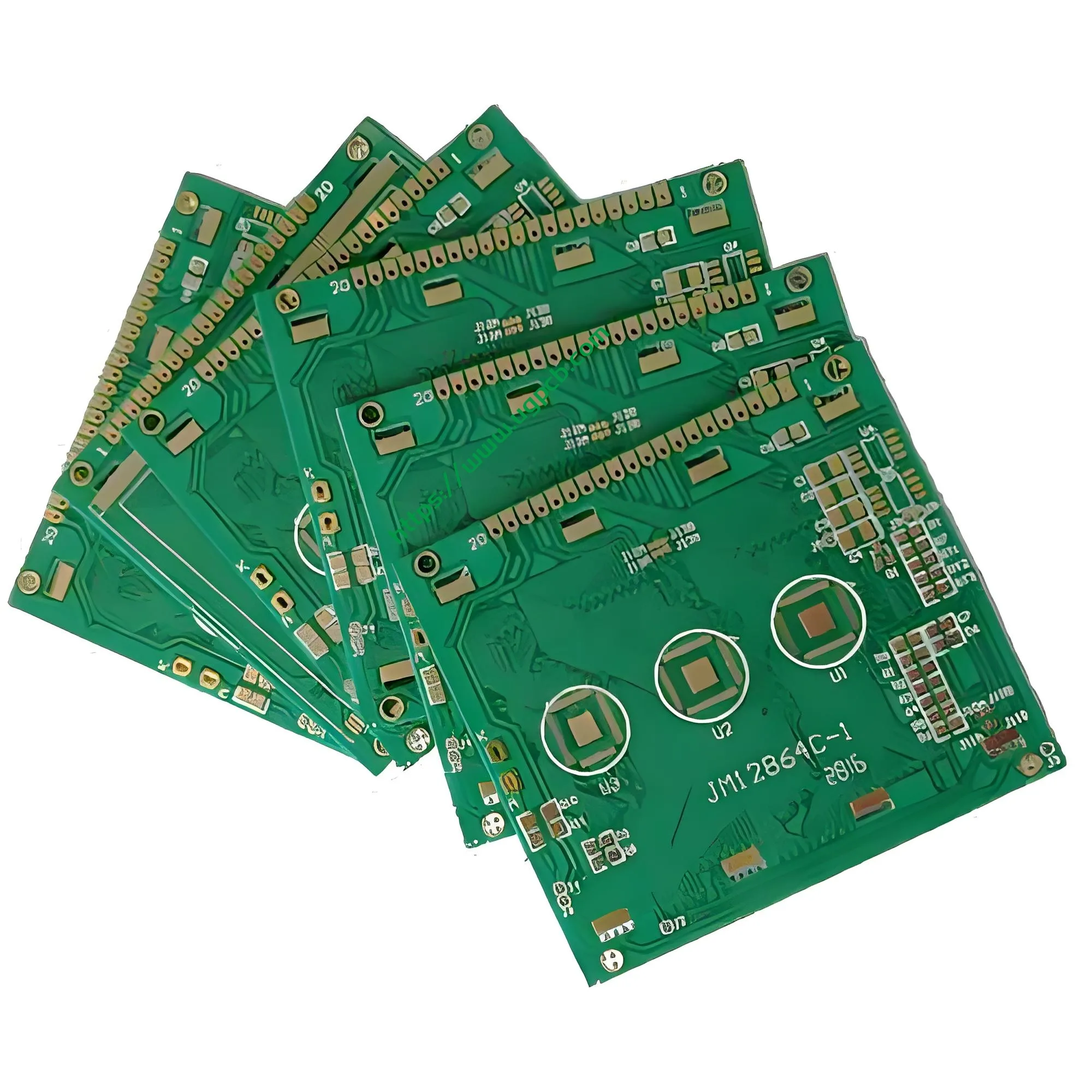
Produktübersicht: Eine hochzuverlässige PCB-Lösung für die Ansteuerung von LCD-Displays
UGPCB stellt die vorLCD-Flüssigkristallanzeige-Leiterplatte (Modell: UGPCB-LCD-001), eine Hochleistungsleistung2-Schicht starre FR-4-Leiterplatte speziell für Anwendungen zur Ansteuerung von Flüssigkristallanzeigen entwickelt. Dieses Produkt verwendet als Basismaterial das hochwertige kupferkaschierte Laminat Kingboard KB6165F, mit einer Plattenstärke von 1.6 mm und 1 Unze Kupferfolie (etwa 35 μm). Die Oberflächenbeschaffenheit beschäftigt sich mit derZUSTIMMEN (Elektrololes Nickel/Immersion Gold) Prozess bei 2U” . Das Brett misst 147.2 × 65 mm, mit einem Mindestlochdurchmesser von 0.22 mm und Mindestlinienbreite/-abstand von 0.3 mm/0,27 mm.
DasLCD-Displayplatine dient als kritischer Schaltkreisträger, der Display-Treiberchips mit Flüssigkristallglasplatten verbindet. Es findet umfangreiche Anwendungen in kleinen bis mittelgroßen LCD-Anzeigemodulen, Industrielle Bedienfeldanzeigen, Displays für Infotainmentsysteme im Automobilbereich, und Smart-Home-Schnittstellen für die Mensch-Maschine-Interaktion.
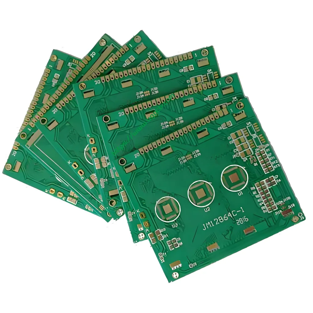
Produktdefinition: Was ist eine LCD-Flüssigkristallanzeige-Leiterplatte??
Ein LCD-Flüssigkristallanzeige-Platine (Leiterplatte) ist eine spezielle Leiterplatte, die für Ansteuersysteme für Flüssigkristallanzeigen entwickelt wurde. Es erfüllt drei Kernfunktionen: Fahrsignalübertragung, Stromverteilung, und Timing-Steuersignal-Routing. Im Gegensatz zum Standard PCB-Leiterplatten, ein LCD-Displayplatine erfordert engere Toleranzen bei der Linienbreitenpräzision, Impedanzkontrolle, und Oberflächenebenheit.
Dieses Produkt gehört zurstarre doppelseitige Leiterplatte Kategorie mit 2 Schichten (2L). Es wird flammhemmendes Material der Güteklasse FR-4 verwendet (UL 94 V-0 bewertet) und unterstützt sowohl SMT (Oberflächenmontagetechnologie) und Durchkontaktierungs-Hybridmontageprozesse für Komponenten. Das Board entspricht der IPC-6012-Klasse 2 Leistungsanforderungen, Dadurch eignet es sich für Anwendungen in der Industrie- und Unterhaltungselektronik.
Designspezifikationen: Kritische Parameter für die Entwicklung von LCD-Leiterplatten
Substratmaterial: Der KB6165F-Vorteil
Dieses Produkt verwendet kupferkaschiertes Laminat Kingboard KB6165F, das die folgenden wichtigen Leistungsmerkmale bietet:
- Glasübergangstemperatur (Tg): ≥150°C, Gewährleistung der Dimensionsstabilität bei bleifreien Reflow-Lötprozessen
- Temperaturtemperatur thermische Zersetzung (Td): 325°C, Bietet eine hervorragende thermische Zuverlässigkeit
- Entflammbarkeitsbewertung: UL 94 V-0, mit selbstverlöschender Flamme im Inneren 10 Sekunden bei vertikalen Brenntests
- CTE (Wärmeleitkoeffizient): 12–15 ppm/°C in X-Y-Richtung, 40–230 ppm/°C in Z-Richtung, Bietet eine gute thermische Anpassung an LCD-Treiber-ICs
- CAF (Leitfähiges anodisches Filament) Widerstand: Hervorragende Anti-CAF-Leistung sorgt für langfristige Zuverlässigkeit
- Bleifrei kompatibel: Erfüllt die RoHS-Umweltanforderungen
Gemäß IPC-2221-Designstandards, Materialien mit Tg ≥150°C sind für bleifreie Montageprozesse geeignet, ist in der Lage, die strukturelle Integrität bei Spitzentemperaturen beim Reflow-Löten von 245–260 °C aufrechtzuerhalten.
Schichtanzahl und Stapeldesign
Die Produkteigenschaften 2 Schichten (2L) mit einem Standard 1.6 mm Plattenstärke. Für IPC-2221, 1.6 mm stellt die am häufigsten verwendete Dickenspezifikation für starre Platten dar Leiterplatten, Balance zwischen mechanischer Festigkeit und einfacher Montage.
Linienbreite und Abstandsdesign
Die minimale Linienbreite von 0.3 mm und einem Mindestzeilenabstand von 0.27 mm sind sorgfältig ausgewählte Parameter fürLCD-Treiberplatine Signalintegrität. Gemäß IPC-2221-Standards, die Mindestabstandsanforderung für konventionelle Spannung (≤30V) digitale Signalspuren ist 0.1 mm (4 Mil). Dieses Produkt 0.27 mm (etwa 10.6 Mil) Der Abstand übersteigt die IPC-Mindestanforderung bei weitem, Bietet ausreichend Spielraum für die Signalqualität.
Referenz zur Entwurfsberechnung (Basierend auf der vereinfachten Formel für die Strombelastbarkeit des Außenschichtleiters IPC-2221):
Strombelastbarkeit der Außenschicht: ≈ k × ΔT^0,448 × W^0,725 × T^0,725
Wobei k = 0.048 (für Außenschicht). Bei einem Temperaturanstieg von 10°C, A 0.3 mm Spur mit 1 Die Kupferdicke von 50 g liefert eine theoretische Strombelastbarkeit von etwa 1,2–1,5 A – ausreichend für die Leistungs- und Signalverfolgungsanforderungen herkömmlicher LCD-Treiberplatinen.
Mindestlochdurchmesser
Der minimale Lochdurchmesser von 0.22 mm (etwa 8.7 Mil) fällt in die Kategorie Präzisionsbohren. Unter IPC-6012, Die Standardtoleranz für den Bohrlochdurchmesser beträgt ±0,08 mm (ca. ±3 Mio) . Für 0.22 mm Mikrovias, Fertigungstoleranzen werden typischerweise innerhalb von ±0,05 mm kontrolliert.
Oberflächenbeschaffung: STIMME zu, dass 2U”
DerZUSTIMMEN (Elektrololes Nickel/Immersion Gold) Oberflächenfinish mit 2U” Golddicke (etwa 0.05 μm) entspricht den IPC-4552-Anforderungen. IPC-4552 Revision A (ausgestellt in 2017) Gibt die Dicke der Goldablagerung an 0.04 μm zu 0.10 μm (1.6 μin zu 4.0 min) und Nickeldicke von 3 μm zu 6 μm.
Vorteile der ENIG-Oberflächenbeschaffenheit:
- Hervorragende Lötbarkeit, unterstützt mehrere Reflow-Zyklen
- Starke Drahtbondfähigkeit
- Überlegene Oxidations- und Korrosionsbeständigkeit
- Flache Oberfläche, geeignet für die Montage von Fine-Pitch-Komponenten
- Verlängerte Haltbarkeit
Funktionsprinzip: Signalübertragungsmechanismen der LCD-Display-Leiterplatte
DerPCB für LCD-Flüssigkristallanzeige arbeitet mit zwei Kernfunktionen: Signalübertragung UndStromverteilung.
1. Signalübertragung des Display-Treibers: Zeigt Daten vom Hauptcontroller-Chip an (MCU/SoC) reist durch diePCB-Leiterplatte über Mikrostreifen- oder Streifenleiterbahnen zum LCD-Treiber-IC. Der Treiber-IC wandelt digitale Signale in analoge Graustufenspannungen um, die dann über ausgegeben werdenLeiterplatteDie feinen Spuren führen zu den ITO-Elektroden auf der Flüssigkristallglasplatte, Steuern des Verdrehungswinkels von Flüssigkristallmolekülen, um das angezeigte Bild zu erzeugen.
2. Timing-Steuersignal-Routing: DerLCD-Displayplatine überträgt wichtige Timing-Signale, einschließlich VSYNC (Vertikale Synchronisierung), HSYNC (Horizontale Synchronisierung), DCLK (Pixeluhr), und DE (Datenaktivierung). Die Übertragungsverzögerung und Impedanzanpassung dieser Signale wirken sich direkt auf die Anzeigequalität aus.
3. Energieverwaltungsverteilung: DerLCD-Platine wandelt die Eingangsleistung um (Typischerweise 3.3 V oder 5 V) durch DC-DC-Umwandlungsschaltungen, um die vom LCD-Panel benötigten mehreren Spannungspegel zu erzeugen, einschließlich VGH (Gate-On-Spannung, Typischerweise +15 V zu +30 V), VGL (Gate-Off-Spannung, typischerweise –5 V bis –15 V), und AVDD (analoge Versorgungsspannung).
Produktklassifizierung: LCD-PCB-Kategorien
Leiterplatten für LCD-Flüssigkristallanzeigen können entlang der folgenden Dimensionen klassifiziert werden:
Für Schichtzahl
- Einseitige Bretter: Wird für einfache Segmentcode-LCD-Anzeigen verwendet
- Doppelseitige Bretter (2L): Die Kategorie dieses Produkts, Wird für kleine bis mittelgroße TFT-LCD-Displaytreiber verwendet
- Mehrschichtplatten (4L und höher): Wird für hohe Auflösung verwendet, großformatige Anzeigemodule
Nach Oberflächenbeschaffenheit
- ENIG-Boards: Die Kategorie dieses Produkts, bietet die beste Gesamtleistung
- OSP-Boards: Niedrigere Kosten, Geeignet für Unterhaltungselektronik mit kurzer Lebensdauer
- HASL-Boards: Geeignet für LCD-Treiberplatinen mit größeren Pinabständen
Durch Anwendung
- LCD-Leiterplatten für Unterhaltungselektronik: Sekundäre Smartphone-Displays, Smartwatch-Displays, E-Reader-Bildschirme
- LCD-Leiterplatten für industrielle Steuerungen: Industrielles HMI, Anzeigen auf der Instrumententafel, Treiber für CNC-Bedienfeldanzeigen
- Automobil-LCD-Leiterplatten: Infotainmentsysteme im Fahrzeug, digitale Kombiinstrumente, HUD-Display-Steuerplatinen
- LCD-Leiterplatten für medizinische Geräte: Patientenmonitore, Ultraschall-Diagnosegeräte, Display-Treiberplatinen für medizinische Bildgebungssysteme
Kernleistungsspezifikationen
| Parameter | Spezifikation | Referenzstandard |
|---|---|---|
| Laminatmaterial | KB6165F (Kingboard) | - |
| Laminattyp | FR-4 Kupferbeschichtetes Laminat aus Glasgewebe | UL 94 V-0 |
| Schichtzahl | 2 Schichten (2L) | - |
| Brettdicke | 1.6 mm | IPC-2221 |
| Kupferdicke der äußeren Schicht | 1 oz (35 μm) | IPC-6012 Klasse 2 |
| Oberflächenbeschaffung | Nur 2 Stunden” (0.05 μm Au) | IPC-4552 |
| Dicke der Nickelschicht | 3–6 μm (Unterschicht) | IPC-4552 Rev A |
| Mindestlochdurchmesser | 0.22 mm | IPC-6012 |
| Mindestlinienbreite | 0.3 mm | IPC-2221 |
| Mindestzeilenabstand | 0.27 mm | IPC-2221 |
| Brettabmessungen | 147.2 × 65 mm | - |
| Tg (Glasübergangstemperatur) | ≥150°C | - |
| Td (Temperaturtemperatur thermische Zersetzung) | 325°C | - |
| CTE (X-Y-Richtung) | 12–15 ppm/°C | - |
| Entflammbarkeitsbewertung | UL 94 V-0 | UL 94 |
| Bogenwiderstand | ≥60 Sekunden | - |
| Oberflächenwiderstand | ≥2,6 × 10⁸ MΩ | - |
| Volumenwiderstand | ≥3,4 × 10⁹ MΩ·cm | - |
Produktstrukturanalyse
DerPCB für LCD-Flüssigkristallanzeige Die Struktur besteht von außen nach innen aus den folgenden Schichten:
1. Äußere Schicht – ENIG-Oberflächenfinish: Goldschicht bei 2U” (etwa 0.05 μm) schützt die darunter liegende Nickelschicht vor Oxidation. Die untere Nickelschicht von 3–6 μm dient als Diffusionsbarriere zwischen Kupfer und Gold.
2. Kupferfolienschicht: 1 oz (etwa 35 μm) galvanisch abgeschiedene Kupferfolie, geätzt, um das Schaltkreismuster zu bilden.
3. Dielektrische Schicht: Mit Epoxidharz imprägniertes Glasgewebe der Güteklasse FR-4, etwa 0.7 mm dick (Einzelschicht), Bereitstellung elektrischer Isolierung und mechanischer Unterstützung.
4. Kupferfolienschicht: Untere Schicht 1 Unzen Kupfer bilden das untere Schaltkreismuster.
5. Äußere Schicht – ENIG-Oberflächenfinish: Symmetrische ENIG-Behandlung passend zur Deckschicht.
Produktmerkmale: Warum sollten Sie sich für die LCD-Display-Leiterplatte von UGPCB entscheiden??
① Hochpräzise Fertigung: Mindestlochdurchmesser von 0.22 mm und Mindestlinienbreite/-abstand von 0.3 mm/0,27 mm unterstützen die Routing-Anforderungen von LCD-Treiberplatinen mit hoher Dichte.
② Premium-Substratmaterialien: Kingboard KB6165F High-End-FR-4-Material mit Tg ≥150 °C und UL 94 V-0 Die Entflammbarkeitsbewertung gewährleistet bleifreie Prozesskompatibilität und langfristige Zuverlässigkeit.
③ Standardisierte Oberflächenbeschaffenheit: Nur 2 Stunden” Der Prozess entspricht IPC-4552, sorgt für eine hervorragende Lötbarkeit, Oxidationsbeständigkeit, und verlängerte Haltbarkeit.
④ Strenge Qualitätskontrolle: Die Produkte unterliegen einer umfassenden Qualitätskontrolle gemäß IPC-6012-Klasse 2 Standards, Toleranz des Lochdurchmessers abdecken (±0,08 mm), Lochkupferdicke (≥20 μm), Integrität der Lötmaske, und elektrische Prüfungen.
⑤ LCD-optimiertes Design: Impedanzkontrolle, Signalintegrität, und Leistungsintegrität sind speziell für Anwendungen zur Ansteuerung von Flüssigkristallanzeigen optimiert.
Herstellungsprozess: Vom Rohstoff bis zum fertigen Produkt
UGPCB folgt einem strengen Standardherstellungsprozess fürLCD-Display-Leiterplatten:
1. Materialschnitt →2. Musterübertragung der inneren Schicht (Bohrpositionierungs- und Registrierungsmarkierungen) →3. Bohren (Mindestlochdurchmesser 0.22 mm ± 0.08 mm) →4. Stromlose Kupferabscheidung/Galvanik (Lochmetallisierung, Lochkupferdicke ≥20 μm) →5. Musterübertragung der äußeren Schicht (Linienbreite 0.3 mm / Abstand 0.27 mm) →6. Musterbeschichtung (Kupferansammlung zu 1 oz) →7. Radierung →8. Lötmaskendruck →9. ENIG-Oberflächenfinish (ZUSTIMMEN, Goldstärke 2U”) →10. Profilierung (Abmessungen 147.2 × 65 mm) →11. Elektrische Tests (100% elektrische Prüfung) →12. Endinspektion (AOI + visuelle Inspektion) →13. Verpackung und Versand
Typische Anwendungsszenarien
📱 Unterhaltungselektronik: Sekundäre Smartphone-Displays, Smartwatch-Displays, E-Reader-Bildschirmtreiberplatinen.
🏭 Industrielle Steuerung: SPS-Mensch-Maschine-Schnittstellen (HMI), Displays für Industrieinstrumente, Treiberplatinen für CNC-Bedienfeldanzeigen.
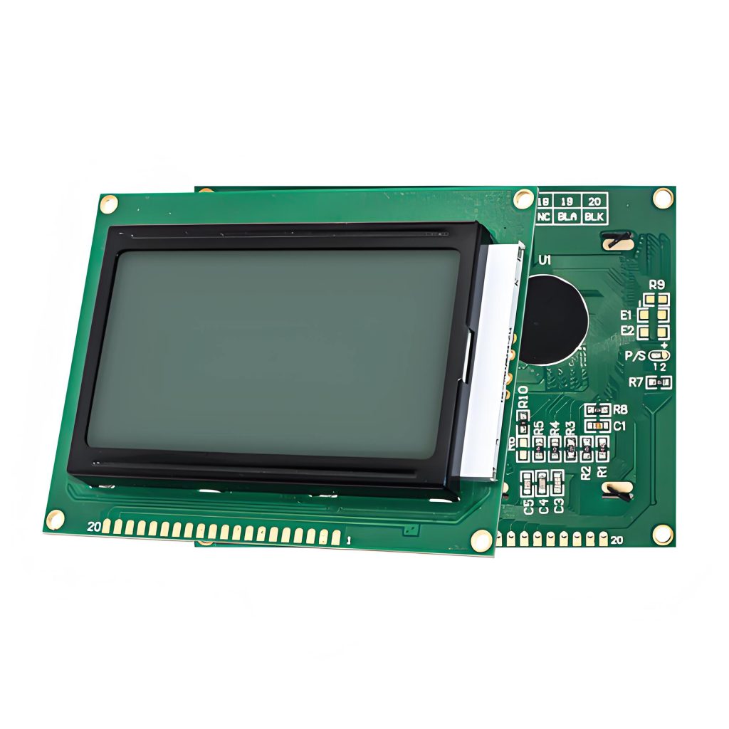
🚗 Automobilelektronik: Infotainmentsysteme im Fahrzeug, digitale Kombiinstrumente, Head-up-Display (HUD) Display-Steuerplatinen.
🏥 Medizinische Geräte: Patientenmonitore, Ultraschall-Diagnosegeräte, Display-Treiberplatinen für medizinische Bildgebungssysteme.
🏠 Smart Home: Intelligente Zutrittskontrollsystem-Anzeigen, Bedienfelder für intelligente Geräte, Leiterplatten für Anzeigemodule für Gebäude-Gegensprechanlagen.
Warum wählen Sie UGPCB??
UGPCB bringt Jahre LCD-Displayplatine Fertigungserfahrung für jedes Projekt. Wir verwenden erstklassige Rohstoffe wie Kingboard KB6165F, IPC-6012-Klasse strikt durchsetzen 2 Qualitätsstandards, und bedienen Sie hochpräzise Bohr- und Schaltungsstrukturierungsgeräte. Ob Sie brauchen LCD PCB -Prototyping oder Massenproduktion, UGPCB liefert hohe Präzision, hochzuverlässige Produktlösungen.
📞 Holen Sie sich noch heute Ihre PCB-Lösung für LCD-Displays
UGPCB Leiterplatten für LCD-Flüssigkristallanzeigen wurden in zahlreichen Industriezweigen erfolgreich eingesetzt, Automobil, und Unterhaltungselektronik-Display-Projekte. Ob Sie brauchen LCD-PCB-Prototyping zur Designvalidierung bzw Leiterplatte schlüsselfertige Montagedienstleistungen, UGPCB bietet umfassende Prozessunterstützung von der Leiterplattenfertigung bis hin zu Leiterplatte SMT -Baugruppe.
Kontaktieren Sie noch heute das professionelle Team von UGPCB für Ihre individuelle LCD-Display-PCB-Lösung!
📧 E-Mail: [info@ugpcb.com]
📞 Telefon: [+86-755-XXXXXXXX]
🌐 Website: [www.ugpcb.com]
Zuordnung der Datenquelle
Die in diesem Dokument zitierten technischen Standards und Daten stammen aus den folgenden maßgeblichen Quellen:
- IPC-6012 - -Qualifikations- und Leistungsspezifikation für starre Leiterplatten – Definiert Toleranzen für den PCB-Lochdurchmesser (Standard ±0,08 mm), Lochkupferdicke (Klasse 2 ≥20 μm), und Leistungsklassenanforderungen
- IPC-2221 - -Allgemeiner Standard für Leiterplattendesign – Spezifiziert Anforderungen an die Linienbreite/-abstände und Berechnungsformeln für die Strombelastbarkeit
- IPC-4552 Revision A (ausgegeben 2017) - -Leistungsspezifikation für chemisches Nickel/Immersionsgold (ZUSTIMMEN) Beschichtung für Leiterplatten – Gibt die Anforderungen an die ENIG-Ablagerungsdicke an: Nickel 3–6 μm, Gold 0,04–0,10 μm
- UL 94 - -Norm zur Sicherheit und Entflammbarkeit von Kunststoffmaterialien für Teile in Geräten und Geräten – V-0 Die Bewertung erfordert eine selbstverlöschende Flamme im Inneren 10 Sekunden
- Kingboard KB6165F Produktdatenblatt – Technische Parameter des Untergrundes (Tg ≥150°C, Td 325°C, UL 94 V-0, usw.)
- GB/T 4677 - -Testmethoden für Leiterplatten – Wird in Verbindung mit IPC-Standards als Inspektionsreferenz verwendet













