

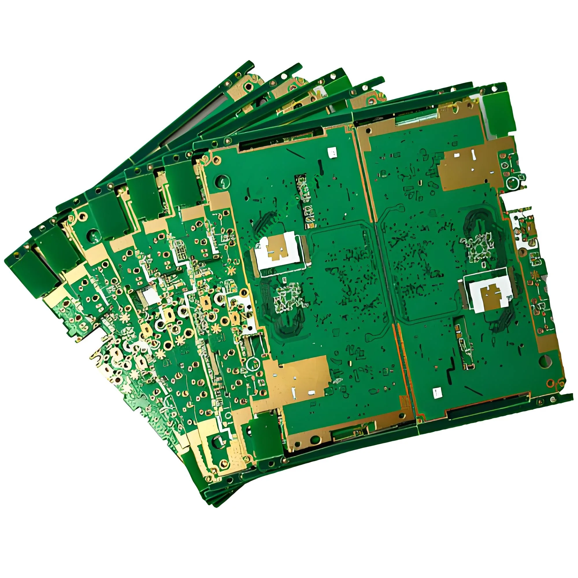
ICH. Produktübersicht: Eine Leiterplatte, die für drahtlose Türklingelsysteme entwickelt wurde
Die Leiterplatte der drahtlosen Türklingel ist eine wesentliche elektronische Komponente in Smart Home- und Sicherheitssystemen. UGPCB bietet dieses Board mit kupferkaschiertem Hochleistungslaminat Kingboard KB6165F an. Der Herstellungsprozess unterliegt strengen Qualitätskontrollen.
Diese Leiterplatte für die drahtlose Türklingel ist eine 2-lagige, doppelseitige Platine Leiterplatte. Es hat eine Dicke von 1,0 mm und die folgenden Abmessungen: 79.48 × 35,6 mm. Diese Abmessungen passen perfekt in kompakte Funk-Türklingelgehäuse. Das Board verwendet bleifreies HASL (Heißluftlötes Leveling) Oberflächenbeschaffung. Diese Oberfläche erfüllt die RoHS-Umweltanforderungen und bietet gleichzeitig eine hervorragende Lötbarkeit.
Drahtlose Türklingeln dienen als erste Verteidigungslinie für die Sicherheit Ihres Zuhauses. Die Zuverlässigkeit ihrer Leiterplatten bestimmt direkt die Produktlebensdauer und das Benutzererlebnis. UGPCB ist sich dieser wichtigen Anforderung bewusst. Wir wählen die Materialien sorgfältig aus und kontrollieren jeden Prozessschritt, um hochwertige drahtlose Türklingeln zu liefern Leiterplatten an Kunden weltweit.
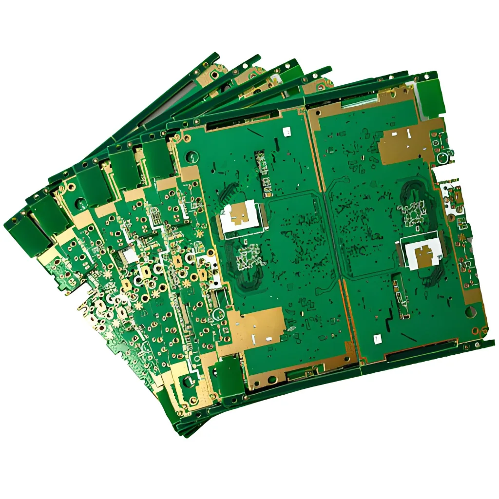
II. Produktdefinition und Branchenpositionierung
ALeiterplatte für drahtlose Türklingel ist eine Leiterplatte, die in drahtlosen Türklingelsystemen verwendet wird. Es besteht typischerweise aus zwei Teilen: eine Senderplatine und eine Empfängerplatine. Die Senderplatine trägt den Encoder-Chip (wie HT12E), ein 433-MHz-Funksendermodul, und der Schaltkreis des Druckknopfschalters. Auf der Empfängerplatine befindet sich der Decoder-Chip (wie HT12D), das Funkempfängermodul, Der Audioverstärker, und die Lautsprechertreiberschaltung.
Aus Sicht der PCB-Klassifizierung, Dieses Produkt ist einstarre doppelseitige Leiterplatte (Starre doppelseitige Leiterplatte) . Es kann wie folgt weiter klassifiziert werden:
| Klassifizierungsdimension | Kategorie |
|---|---|
| Leitfähige Schichten | Doppelseitig (2L) |
| Substratsteifigkeit | Starres Brett |
| Oberflächenbeschaffung | Bleifreies HASL |
| Entflammbarkeitsbewertung | UL 94 V-0 |
| IPC-Leistungsklasse | Klasse 2 (Spezielle Service-Elektronikprodukte) |
Dieses Produkt entspricht IPC-6012Qualifikations- und Leistungsspezifikation für starre Leiterplatten. Sein Substratmaterial, KB6165F, erfüllt die Spezifikationsanforderungen IPC-4101/99.
III. Wichtige technische Parameter
3.1 Substratmaterial: Kingboard KB6165F Kupferkaschiertes Laminat
KB6165F ist einbleifreies, kupferkaschiertes Laminat aus Tg150-Glasgewebe hergestellt von Kingboard Laminates Holdings Limited. Es gehört zur Familie der Epoxidglasgewebelaminate der Güteklasse FR-4. Die wichtigsten Leistungsindikatoren sind wie folgt:
- Glasübergangstemperatur (Tg) : 154°C (Testmethode: IPC-TM-650 2.4.25)
- CTE der Z-Achse (Wärmeleitkoeffizient) : 40 ppm/° C. (50–260°C), totale Expansion 3.1% (Testmethode: IPC-TM-650 2.4.24)
- T-288 Delaminierungszeit : >30 Minuten (Testmethode: IPC-TM-650 2.4.24.1)
- Temperaturtemperatur thermische Zersetzung (Td, 5% Gewichtsverlust) : 346°C (Testmethode: IPC-TM-650 2.4.24.6)
- Entflammbarkeitsbewertung : UL 94 V-0
- Dielektrizitätskonstante (Dk) @ 1GHz : 4.6 (Testmethode: IPC-TM-650 2.5.5.2)
- Dissipationsfaktor (Df) @ 1GHz : 0.016 (Testmethode: IPC-TM-650 2.5.5.2)
- Schalenstärke (1 Unze Kupferfolie) : 1.4 N/mm (Testmethode: IPC-TM-650 2.4.8)
- Biegerstärke : 550 N/mm² (längs) / 485 N/mm² (quer) (Testmethode: IPC-TM-650 2.4.4)
- Feuchtigkeitsabsorption : 0.10% (Testmethode: IPC-TM-650 2.6.2.1)
- Wärmespannung : ≥240 Sekunden (Testmethode: IPC-TM-650 2.4.13.1)
Eine hohe Tg (>150°C) bedeutet, dass dieses Substrat den hohen Temperaturen bleifreier Lötprozesse standhält. Es verhindert wirksam ein Verziehen und Delaminieren der Platine während der Montage. Es ist ein ausgezeichnetes Anti-CAF (Leitfähiges anodisches Filament) Die Leistung gewährleistet Zuverlässigkeit in feuchten Umgebungen und unter langfristigen Einschaltbedingungen.
3.2 Plattendicke und Schichtanzahl
Die Plattenstärke beträgt1.0mm mit2 Schichten (2L) . Diese Dicke bietet ausreichende mechanische Festigkeit und unterstützt gleichzeitig die dünnen und kompakten Designanforderungen drahtloser Türklingelprodukte. Das doppelschichtige Design ermöglicht eine ordnungsgemäße Anordnung der HF-Schaltkreise, Stromkreise, und Steuerkreise sowohl auf der Sender- als auch auf der Empfängerplatine. Dies optimiert die Signalintegrität und die Leistungsintegrität.
3.3 Abmessungen
Die Abmessungen sind79.48mm × 35,6 mm. Diese kompakte Größe ist für den Innenraum drahtloser Türklingelprodukte optimiert. Es beherbergt alle Funktionsschaltkreise und passt problemlos in verschiedene Türklingelgehäuse.
3.4 Minimale Blende
Die minimale Blende beträgt0.332mm. Gemäß IPC-6012-Anforderungen für durchkontaktierte Löcher, Diese Öffnungsgröße erfüllt die Zuverlässigkeitsanforderungen beim Einsetzen von Komponentenleitungen und bei der Metallisierung von Durchkontaktierungen in Leiterplatten für drahtlose Türklingeln.
3.5 Spurenbreite und Abstand
Die Spurbreite beträgt0.42mm und der Spurabstand ist0.46mm. Gemäß IPC-2221Allgemeiner Standard für Leiterplattendesign, Die Strombelastbarkeit kann mit der folgenden Formel berechnet werden:
Wo:
- = Maximale Strombelastbarkeit (Ampere)
- = Korrekturfaktor (0.048 für Außenschichten, 0.024 für Innenschichten)
- = Zulässiger Temperaturanstieg (°C)
- = Leiterquerschnittsfläche (Quadratmillionen)
Für Außenschichtspuren mit 1 Unze Kupferfolie (1.37 Mil dick) und eine Leiterbahnbreite von 0,42 mm (etwa 16.5 Mils), die Querschnittsfläche beträgt:
Bei einem Temperaturanstieg von 10°C, die theoretische Strombelastbarkeit beträgt:
Diese Stromkapazität erfüllt vollständig die Anforderungen von HF-Schaltkreisen mit geringem Stromverbrauch und digitalen Steuerschaltkreisen in Leiterplatten für drahtlose Türklingeln.
3.6 Dicke der Kupferfolie
Die Dicke der Kupferfolie beträgt1/1OZ (1 Unzen auf beiden Außenschichten, ca. 35μm). Diese Dicke sorgt für ein hervorragendes Gleichgewicht zwischen der Strombelastbarkeit, Wärmeleitfähigkeit, und Kosten. Es handelt sich um die Standardkonfiguration für Leiterplatten der Unterhaltungselektronik.
3.7 Oberflächenbeschaffung: Bleifreies HASL
Die Oberflächenbeschaffenheit istbleifreies HASL (Heißluftlötes Leveling) . In diesem Prozess, Die Leiterplatte wird in eine geschmolzene bleifreie Lotlegierung getaucht (typischerweise Sn99,3Cu0,6). Anschließend blasen Hochdruck-Heißluftmesser über die Oberfläche, um überschüssiges Lot zu entfernen.
Zu den Hauptvorteilen der bleifreien HASL-Oberflächenveredelung gehören::
- Hervorragende Lötbarkeit : Geeignet für mehrere Lötzyklen
- Lange Haltbarkeit : Die Lotlegierung sorgt für eine gute Lagerstabilität
- Kosteneffizienz : Wirtschaftlicher als ENIG und andere Oberflächen
- RoHS-Konformität : Enthält kein Blei oder andere eingeschränkte Substanzen
Diese Oberflächenveredelung erfüllt die Beschichtungsanforderungen gemäß IPC-6012.
3.8 Lötmaske und Legende
Die Lötstoppmaske istgrüne Tinte und die Legende istWeiße Tinte. Grüne Lötmasken sind die beliebteste Wahl in der Leiterplattenindustrie. Es bietet hervorragende Isoliereigenschaften, Wärmewiderstand, und visuelle Klarheit. Weiße Legende stellt sicher, dass Komponentenbezeichner, Polaritätsmarkierungen, und andere Informationen bleiben klar lesbar.
IV. Designrichtlinien und Betriebsprinzipien
4.1 Entwurfsrichtlinien
Drahtlose Türklingel PCB-Design erfordert die Aufmerksamkeit auf mehrere kritische Bereiche:
(1) HF-Schaltungsdesign
Drahtlose Türklingeln arbeiten normalerweise im 433-MHz-ISM-Band. HF-Leiterbahnen müssen als Mikrostreifenleitungen mit einer charakteristischen Impedanz von 50 Ω oder als koplanare Wellenleiter ausgelegt sein. Die Leiterbahnbreite muss anhand der genau berechnet werden PCB -Material Parameter (Dk = 4.6). Die Antenne sollte in der Nähe des PCB-Randes platziert werden. Vermeiden Sie es, es in der Mitte der Platine zu platzieren oder es von großen Grundplatten zu umgeben.
(2) Kraftintegrität
Die Energieverwaltungsschaltkreise auf den Sender- und Empfängerplatinen erfordern eine ordnungsgemäße Anordnung. Platzieren Sie Entkopplungskondensatoren in der Nähe der IC-Pins “nah und vielfältig” Prinzip.
(3) Interferenzminderung
Platzieren Sie die Empfängerschaltung in einer Ecke der Platine, Abstand zu Schaltnetzteilen und anderen Störquellen. Die Quarzoszillatorschaltung benötigt eine eigene Masseebene und sollte so nah wie möglich an der MCU platziert werden.
(4) Thermalmanagement
Die Plattenstärke von 1,0 mm kombiniert mit 1 Unzen Kupferfolie sorgt für eine gute Wärmeleitfähigkeit. Dadurch wird die Wärme von HF-Leistungsverstärkern und anderen wärmeerzeugenden Komponenten effektiv abgeleitet.
4.2 Funktionsprinzipien
Ein drahtloses Türklingelsystem besteht aus einem Sender und einem Empfänger:
Senderbetrieb : Wenn ein Benutzer die Türklingeltaste drückt, Der Encoder-Chip (wie HT12E) auf der Senderplatine kodiert das Tastensignal. Das 433-MHz-HF-Sendemodul sendet dieses codierte Signal dann drahtlos. Der Sender verbraucht im Betrieb typischerweise etwa 5,6 mA.
Empfängerbetrieb : Das 433-MHz-HF-Empfängermodul auf der Empfängerplatine überwacht kontinuierlich Funksignale. Wenn es ein passendes codiertes Signal empfängt, Der Decoder-Chip (wie HT12D) entschlüsselt es. Dadurch wird die Audioverstärkerschaltung aktiviert, um den Lautsprecher anzusteuern und den Türklingelton zu erzeugen.
V. Produktmerkmale und Leistungsvorteile
5.1 Produktmerkmale
| Besonderheit | Beschreibung |
|---|---|
| Hochzuverlässiges Substrat | Kingboard KB6165F Tg150 Laminat, UL 94 V-0 schwer entflammbar |
| Umweltfreundliches bleifreies Verfahren | Bleifreie HASL-Oberflächenveredelung, ROHS -konform |
| Präzisionsfertigungsfähigkeit | Minimale Blende 0,332 mm, unterstützt High-Density-Routing |
| Ausgezeichnete Hitzebeständigkeit | T-288 >30min, widersteht bleifreien Reflow-Löttemperaturen |
| Überlegene elektrische Leistung | Dk=4,6, Df=0,016 bei 1 GHz, geeignet für HF-Anwendungen |
| Hohe Maßgenauigkeit | Präzise Abmessungen von 79,48 x 35,6 mm, Passend für Standard-Türklingelgehäuse |
5.2 Leistungsvorteile
(1) Einhaltung internationaler Standards
Das Produkt wurde gemäß IPC-6012 entwickelt und hergestelltQualifikations- und Leistungsspezifikation für starre Leiterplatten und IPC-A-600Akzeptanz von Leiterplatten. Das Substrat erfüllt die Anforderungen der IPC-4101/99-Spezifikation.
(2) UL-Sicherheitszertifizierung
Das Substrat KB6165F hat die UL-Zertifizierung erhalten (UL-File-Nr. E123995). Seine Flammschutzklasse entspricht UL 94 V-0. Es entspricht auch UL 796Standard für Leiterplatten für starre Platinen, die als Komponenten in Geräten oder Geräten verwendet werden.
(3) Umweltverträglichkeit
Der niedrige CTE der Z-Achse (40 ppm/° C.) und die hervorragende Anti-CAF-Leistung sorgen für langfristige Zuverlässigkeit bei Temperaturschwankungen und feuchten Bedingungen.
VI. Ablauf des Herstellungsprozesses
UGPCB folgt einem standardisierten Herstellungsprozess für Leiterplatten für drahtlose Türklingeln:
① Wareneingangskontrolle → Substrat und Kupferfolie gemäß IPC-A-600 prüfen
② Schaltkreisbildung der inneren Schicht → Trockenfilm laminieren, exponieren, entwickeln, und ätzen, um Schaltkreismuster der inneren Schicht zu bilden
③ Laminierung → Innenschichtkerne mit Prepreg laminieren (Pp) unter hoher Temperatur und hohem Druck
④ Bohren → CNC Bohren, minimale Blende 0,332 mm
⑤ Stromlose Kupferabscheidung / Plattenbeschichtung → Stromlose Kupferabscheidung + Vollflächige Galvanisierung für die elektrische Verbindung zwischen den Schichten
⑥ Schaltkreisbildung der äußeren Schicht → Laminatfolie, exponieren, entwickeln, Musterplatte, und ätzen, um äußere Schaltkreise zu bilden
⑦ Auftragen einer Lötmaske → Tragen Sie grüne Lötmaskentinte auf, um Schaltkreise zu schützen und Lötkurzschlüsse zu verhindern
⑧ Oberflächenbeschaffenheit → Bleifreies HASL (Heißluftlötes Leveling)
⑨ Legendendruck → Weiße Legende drucken, um Komponentenbezeichner zu identifizieren
⑩ Routing → CNC-Fräsen oder Stanzen auf die endgültigen Abmessungen von 79,48 x 35,6 mm
⑪ Elektrische Prüfung → Fliegende Sonde oder Vorrichtungstests für 100% Unterbrechungs-/Kurzschlusserkennung
⑫ Endkontrolle → Sicht- und Maßprüfung gemäß IPC-A-600
⑬ Verpackung und Versand → Vakuumverpackung mit Feuchtigkeitsschutz
VII. Anwendungsszenarien und Endverbrauchsmärkte
Leiterplatten für drahtlose Türklingeln werden häufig in den folgenden Anwendungen verwendet:
| Anwendungsszenario | Beschreibung |
|---|---|
| Drahtlose Türklingeln für Privathaushalte | Haustürklingelsysteme mit Sender im Freien und Empfänger im Innenbereich |
| Intelligente Gebäude-Gegensprechanlagen | Drahtlose Rufeinheiten für Zutrittssysteme in Mehrfamilienhäusern |
| Hotelservice-Rufsysteme | Drahtlose Sendemodule für Ruftasten für den Hotelzimmerservice |
| Notrufsysteme für die Altenpflege | Drahtlose Senderplatinen für Notruftasten für Senioren |
| Smart Home IoT-Geräte | Intelligente Türklingeln mit integrierten WLAN-Modulen |
| Sicherheits- und Überwachungssysteme | Drahtlose Auslöse- und Alarmeinheiten für Sicherheitsausrüstung |
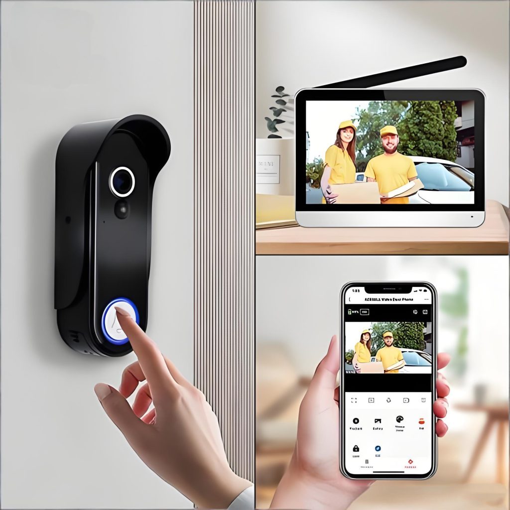
Leiterplatten für drahtlose Türklingeln sind Kernkomponenten in der Unterhaltungselektronik und in Smart-Home-Geräten. Die Marktnachfrage wächst weiter. Da die Einführung von Smart Homes immer schneller voranschreitet, das Bedürfnis nach hoher Qualität, Die Zahl hochzuverlässiger Leiterplatten für drahtlose Türklingeln nimmt rasant zu.
VIII. Warum sollten Sie sich für UGPCB-Leiterplatten für drahtlose Türklingeln entscheiden??
✅ Premium-Substratmaterial : Kingboard KB6165F Tg150 Laminat mit UL 94 V-0 Flammschutz gewährleistet Produktsicherheit und Zuverlässigkeit
✅ Einhaltung internationaler Standards : Design und Fertigung entsprechen IPC-6012, IPC-A-600, IPC-2221, und andere internationale Spezifikationen
✅ Umweltfreundliches bleifreies Verfahren : Die bleifreie HASL-Oberflächenveredelung erfüllt die RoHS-Umweltanforderungen
✅ Präzisionsfertigungsfähigkeit : Minimale Blende 0,332 mm, Leiterbahnbreite/-abstand 0,42/0,46 mm für hochpräzise Routing-Anforderungen
✅ Professioneller RF-Design-Support : 50Ω-Impedanzkontrolle und andere professionelle Designunterstützung für drahtlose 433-MHz-Türklingelanwendungen
✅ Schnelle Lieferung : Prototypen in 4–5 Tagen mit beschleunigten Optionen verfügbar
IX. Anfrage- und Bestellleitfaden
UGPCB ist bestrebt, qualitativ hochwertige Leiterplatten für drahtlose Türklingeln bereitzustellen Leiterplatte schlüsselfertige Dienstleistungen für Kunden weltweit. Ganz gleich, ob Sie als Hardware-Ingenieur ein neues drahtloses Türklingelprodukt entwickeln oder als Beschaffungsmanager auf der Suche nach einem zuverlässigen Leiterplattenlieferanten sind, UGPCB ist Ihr vertrauenswürdiger Partner.
Fordern Sie noch heute ein Angebot an, um exklusive Preise und engagierten technischen Support zu erhalten.
📧E-Mail : info@ugpcb.com
🌐Webseite : www.ugpcb.com
Bitte stellen Sie Ihre PCB-Designdateien zur Verfügung (Gerber-Dateien), Materialversorgungsrechnung (Stückliste), und alle besonderen Prozessanforderungen. Das professionelle UGPCB-Team wird innerhalb von 24 Stunden antworten 24 Stunden mit einer optimierten PCB/PCBA-Lösung.
Datenquellendeklaration
Die in diesem Dokument genannten technischen Daten stammen von den folgenden maßgeblichen Organisationen und Standards:
- Kingboard Laminates Holdings Limited : Technisches Datenblatt für kupferkaschiertes Laminat KB-6165F
- IPC – Association Connecting Electronics Industries : IPC-6012 Qualifikations- und Leistungsspezifikation für starre Leiterplatten
- IPC – Association Connecting Electronics Industries : IPC-A-600 Akzeptanz von Leiterplatten
- IPC – Association Connecting Electronics Industries : IPC-2221 Allgemeiner Standard für Leiterplattendesign
- IPC – Association Connecting Electronics Industries : IPC-TM-650 Handbuch zu Testmethoden (2.4.4, 2.4.8, 2.4.13.1, 2.4.24, 2.4.24.1, 2.4.24.6, 2.4.25, 2.5.5.2, 2.6.2.1)
- UL – Underwriters Laboratories : UL 796 Standard für Leiterplatten
- UL – Underwriters Laboratories : UL 94 Norm für Tests zur Entflammbarkeit von Kunststoffmaterialien für Teile in Geräten und Geräten













