

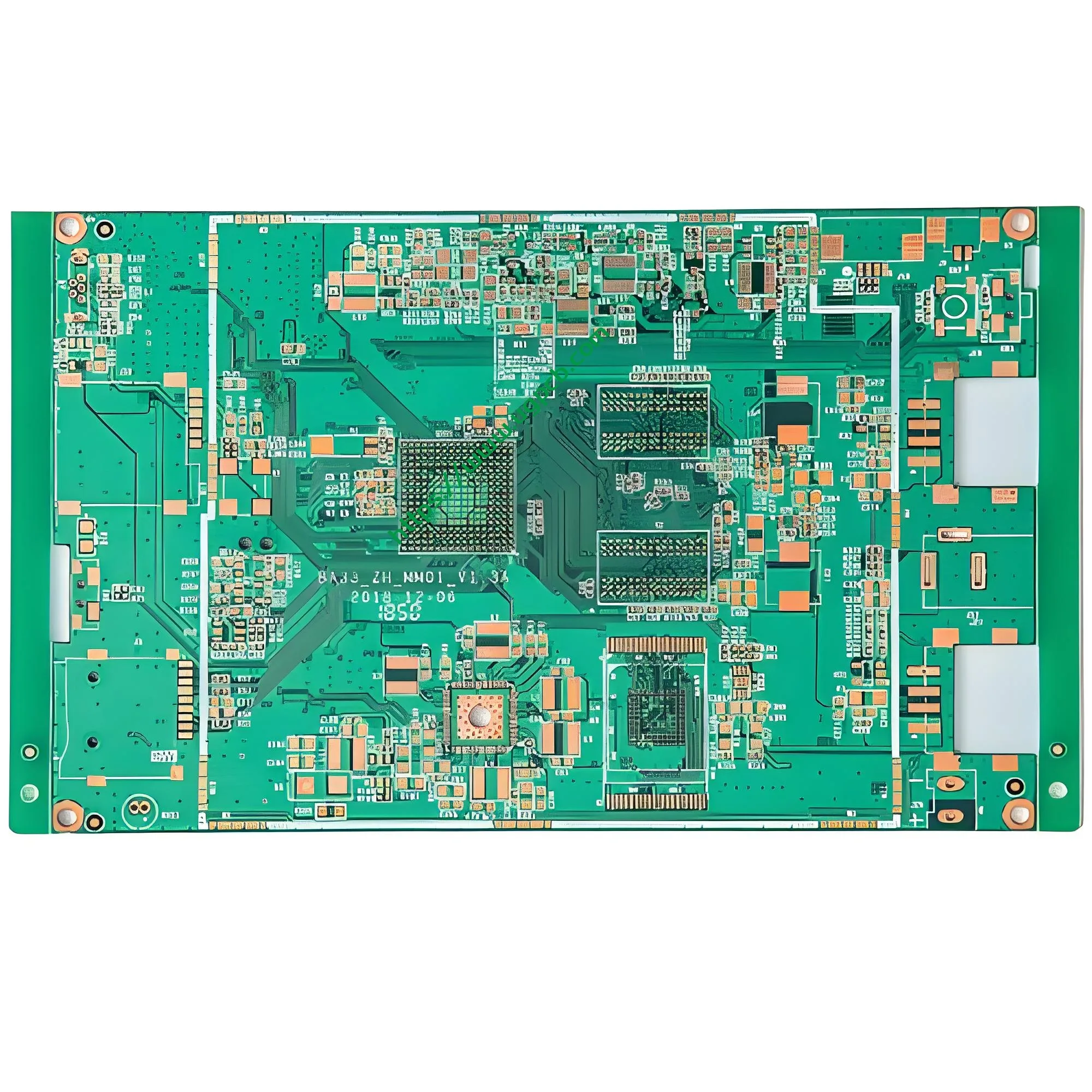
Produktübersicht: Was ist eine OSP-Antioxidans-PCB-Leiterplatte??
EinOSP-Antioxidans-PCB-Leiterplatte verwendetBio -Lötbarkeitskonservierungsmittel (OSP) ebenso wie die Kupferoberfläche. Bei diesem Verfahren wird ein ultradünner organischer Film auf blanken Kupferoberflächen abgeschieden. Die Folie verhindert Oxidation während der Lagerung und Montage. Beim Löten, Das Flussmittel löst den OSP-Film schnell auf. Dadurch wird sauberes Kupfer für zuverlässige Lötverbindungen freigelegt.
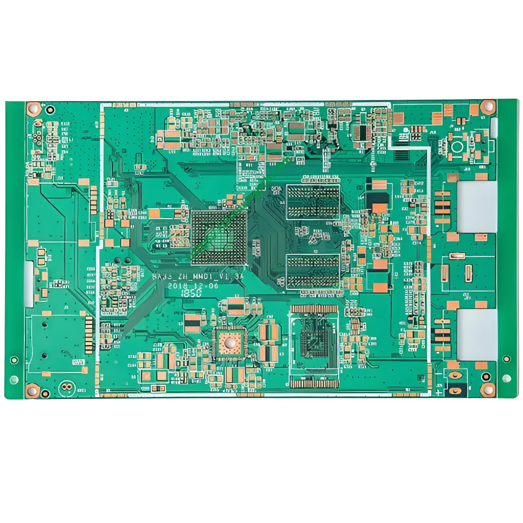
Die antioxidative OSP-Leiterplatte von UGPCB verwendetFR-4-Glasepoxidlaminat als Grundmaterial. Es verfügt über 35 μm (1 oz) Kupferfolie, 1.6mm Plattenstärke, und Abmessungen von 68.36 × 34,6 mm. Die minimale fertige Lochgröße beträgt 0,45 mm. Die minimale Leiterbahnbreite beträgt 0,15 mm und der Mindestabstand 0,20 mm. Das Produkt entspricht vollständig IPC-6012E (Qualifikation und Leistung starrer Leiterplatten) und IPC-4555 (Hochtemperatur-OSP-Leistung) Spezifikationen.
Dasdoppelseitige OSP-Leiterplatte bedient Unterhaltungselektronik, Kommunikationsausrüstung, und industrielle Steuerungen. Es funktioniert am besten dort, wo es auf Kostensensibilität und Oberflächenebenheit ankommt.
Wissenschaftliche Produktklassifizierung
Basierend auf internationalen PCB-Klassifizierungssystemen, Dieses Produkt fällt in diese Kategorien:
| Klassifizierungsdimension | Kategorie |
|---|---|
| Substratmaterial | Starre Leiterplatte aus FR-4-Epoxidglasgewebe |
| Anzahl der Schichten | Doppelseitig (zweischichtige Schaltung) |
| Oberflächenbeschaffung | OSP (Bio -Lötbarkeitskonservierungsmittel) Antioxidans |
| Entflammbarkeitsbewertung | UL 94 V-0 |
| IPC-Leistungsklasse | Klasse 2 (dedizierter Service für elektronische Produkte) |
| Dicke der Kupferfolie | 1 oz (35μm) Standardkupfer |
| Brettdicke | 1.6mm starre Standardplatte |
| Lochtyp | Durchgangsbohrung kompatibel mit SMT |
Wichtige technische Parameter erklärt
Substrat: FR-4 Epoxidglasgewebe
FR-4 ist das am häufigsten verwendete starre Substrat in der Welt Leiterplatte Industrie. “FR” bedeutet flammhemmend. “4” weist darauf hin, dass Epoxidharz mit Glasgewebe kombiniert istUL 94 V-0 Entflammbarkeitsnormen. UL 94 V-0 erfordert, dass vertikale Proben im Inneren selbstverlöschen10 Sekunden nach zwei 10-sekündigen Flammenanwendungen. Keine brennenden Tropfen dürfen Baumwolle entzünden.

Die Glasübergangstemperatur (Tg) misst die Hitzebeständigkeit. Der Standard-FR-4-Tg-Bereich liegt zwischen 130 und 140 °C. FR-4 mit mittlerer Tg erreicht 150–160 °C. FR-4 mit hoher Tg übersteigt 170 °C. Dieses Produkt verwendet Standard-FR-4 mit Tg ≥ 130 °C (IPC-4101/21-konform). Dies erfüllt die Thermoschockanforderungen des Reflow-Lötens (Spitzentemperaturen 240–260°C).
Dicke der Kupferfolie: 35μm (1 oz)
Die Kupferdicke bestimmt die Strombelastbarkeit. Dieses Produkt verwendet35μm Kupferfolie, bekannt als1 Oz Kupfer (1 oz/ft² ≈ 35μm). Gemäß IPC-2221, 1 Unzen Kupfer bei einem Temperaturanstieg von 10°C tragen ungefähr:
- 0.15mm (6 Mil) Spurenbreite: 0.5-0,7A
- 0.20mm (8 Mil) Spurenbreite: 0.8-1,0A
Die Kupferdicke von 35 μm ist der gebräuchlichste Standard für doppelseitige Leiterplatten. Es gleicht die Kosten aus, aktuelle Kapazität, und Fertigungsausbeute.
Brettabmessungen: 68.36 × 34,6 mm
Die fertigen Brettmaße68.36mm × 34,6 mm. Diese kompakte Größe eignet sich für enge elektronische Module. Kleine Leiterplatten erfordern eine höhere Präzision – Maßtoleranzen liegen typischerweise bei ±0,15 mm (IPC-6012 Klasse 2).
Mindestgröße des fertigen Lochs: 0.45mm
0.45mm ist das minimale durchkontaktierte Loch (PTH) Durchmesser. Diese Lochgröße ist ein Standard in der Branche. Es sorgt für eine zuverlässige Beschichtung (Seitenverhältnis ungefähr 3.6:1 mit 1,6mm Plattenstärke). Die Lochgröße bietet Platz für die meisten DIP-Komponenten und Standard-SMT-Pad-Designs.
PCB-Dicke: 1.6mm
1.6mm ist die häufigste Leiterplattendicke bei der Leiterplattenherstellung. Es bietet hervorragende mechanische Festigkeit und Biegesteifigkeit. Es passt perfekt zu Standardsteckern und -buchsen.
Spurenbreite und Abstand: 0.15mm / 0.20mm
Dieses Produkt bietetMindestspurbreite von 0,15 mm (um 6 Mils) UndMindestabstand von 0,20 mm (um 8 Mils). Gemäß IPC-Klassifizierung, Diese Dimensionen fallen inKlasse 2 (dedizierter Service für elektronische Produkte). Diese Präzision erfüllt die meisten PCB-Designs mittlerer Dichte, einschließlich MCU-Steuerplatinen, Energieverwaltungsmodule, und Schnittstellenkonverterplatinen.
Wie der OSP-Antioxidationsprozess funktioniert
Beim OSP-Prozess entsteht ein ultradünner organischer Film auf sauberem, blankem Kupferchemische Adsorption. Der OSP-Film besteht hauptsächlich ausAlkylbenzimidazolverbindungen (auf Azolbasis). Die Filmdicke liegt typischerweise im Bereich von0.2–0,5μm.
Schutzmechanismus
Die OSP-Folie schützt Kupferoberflächen durch drei Mechanismen:
- Physische Barriere – Der organische Film bildet eine dichte Molekülschicht. Es verhindert, dass Sauerstoff und Feuchtigkeit mit der Kupferoberfläche in Kontakt kommen.
- Chemische Adsorption – Aktive Gruppen in OSP-Molekülen verbinden sich chemisch mit Kupferatomen. Dadurch entsteht eine starke Haftung.
- Selektiver Schutz – Die OSP-Folie deckt nur Kupferbereiche ab. Es wirkt sich nicht auf Lötstopplack oder andere nichtmetallische Bereiche aus.
Verhalten beim Löten
Beim SMT-Reflow, Temperaturen erreichen190–230°C. Die Wirkstoffe des Flussmittels zersetzen und lösen den OSP-Film auf. Dadurch wird sauberes Kupfer darunter freigelegt. Das Lot berührt blankes Kupfer direkt und formt esintermetallische Verbindungen (IMC). Dadurch entstehen zuverlässige elektrische Verbindungen. Der OSP-Filmzersetzt sich vollständig ohne Rückstände nach dem Löten.
Wichtige Leistungsmerkmale
Basierend auf IPC-TM-650-Testmethoden:
| Merkmal | Typischer Wert / Erfordernis | Referenzstandard |
|---|---|---|
| OSP-Foliendicke | 0.2–0,5μm | IPC-4555 |
| Lotbenetzungswinkel | ≤30° (nach 1 Reflow) | IPC-TM-650 2.4.1 |
| Lotausbreitungsverhältnis | ≥80 % | IPC-TM-650 2.4.1 |
| Oxidationsschutz (Umgebung) | ≥6 Monate | IPC-4555 |
| Kontaktwiderstandsänderung | ≤10 % (nach 6 Monate Lagerung) | IPC-TM-650 |
OSP-Antioxidans-PCB-Herstellungsprozess
Die Herstellung von OSP-Antioxidations-PCBs folgt strengen Prozesskontrollen. Jeder Schritt beeinflusst die Endqualität und Zuverlässigkeit.
Front-End-Prozesse (Untergrundvorbereitung & Schaltungsstrukturierung)
- Materialschnitt – Schneiden Sie das kupferkaschierte FR-4-Laminat zu
- Bohren – CNC-Bohren mit einer Mindestlochgröße von 0,45 mm
- Chemisches Kupfer / Galvanisieren – Metallisieren Sie die Lochwände für eine Schicht-zu-Schicht-Verbindung
- Schaltungsmusterübertragung – Trockener Film / Nassfilmbelichtung und -entwicklung
- Radierung – Entfernen Sie unerwünschtes Kupfer, um eine 0,15-mm-Leiterbahn zu erzeugen / 0.20Schaltkreise mit mm-Abstand
- Lötmaskendruck – Tragen Sie grüne oder andersfarbige Lötstopplacktinte auf
- Vorreinigung – Entfernen Sie Oxide und Verunreinigungen vor der Oberflächenbearbeitung
OSP-Beschichtungsprozess (Kernprozess)
Der typische OSP-Beschichtungsverlauf:
Entfettung → Doppelte Wasserspülung → Mikroätzung → Doppelte Wasserspülung → Säurebeizen → DI-Wasserspülung → OSP-Filmbildung → Lufttrocknung → DI-Wasserspülung → Endtrocknung
- Mikroätzung – Entfernt Kupferoxide und erzeugt eine gleichmäßige, mikroskopisch raue Oberfläche. Dies fördert das Wachstum des OSP-Films.
- OSP-Filmbildung – Tauchen Sie die Leiterplatte in die OSP-Chemie ein (Alkylbenzimidazol, organische Säuren, Kupferchlorid, und entionisiertes Wasser). Der Film wächst durch chemische Adsorption auf Kupferoberflächen.
- Kontrolle der Filmdicke – Präzise Kontrolle ist entscheidend. Zu dünn bedeutet schlechte Hitzebeständigkeit. Zu dick behindert die Flussmittelwirkung und den Lotfluss.
Back-End-Prozesse
- Routenführung – CNC-Fräsen auf Endmaße
- Elektrische Tests – Flying-Probe- oder Fixture-Tests
- Endinspektion – Sichtprüfung und Schichtdickenprobenahme
- Vakuumverpackung – Feuchtigkeits- und oxidationsbeständige Verpackung
Produktmerkmale und Hauptvorteile
Ausgezeichnete Oberflächenebenheit
Der OSP-Film ist nur0.2–0,5μm dick. Es bildet sich durch chemische Adsorption mit gleichmäßiger Dicke und glatter Oberfläche. Dadurch bleibt die ursprüngliche Ebenheit der Kupferfolie erhalten. Es ist ideal fürFine-Pitch-SMT Komponenten (wie QFP mit einem Rastermaß von 0,4 mm und weniger, QFN-Pakete).
Hervorragende Lötbarkeit
Der OSP-Film löst sich beim Reflow schnell im Flussmittel auf. Dadurch wird frisches Kupfer für eine zuverlässige IMC-Bildung freigelegt. Der OSP-Prozess unterstützt beidesDurchgangsloch (Tht) UndOberflächenmontage (SMT) Löten.
Kostengünstig
OSP verwendet keine Edelmetalle (Gold, Silber, Palladium). Material- und Verarbeitungskosten sind niedriger als bei ENIG, Eintauchen Silber, oder Tauchdose. Für die Massenproduktion wie Unterhaltungselektronik, OSP bietet eine außergewöhnliche Kostenwettbewerbsfähigkeit.
Umweltkonform
OSP verwendet organische Verbindungen. Es enthält kein Blei, Quecksilber, Cadmium, oder sechswertiges Chrom. Es erfüllt voll und ganzRoHS 2.0 Anforderungen. Auch die Kosten und die Komplexität der Abfallbehandlung sind geringer als bei Metallveredelungsprozessen.
Kurze Bearbeitungszeit
Die OSP-Beschichtung ist einfach und schnell. Es sind weder komplexe Beschichtungsgeräte noch lange Abscheidungszeiten erforderlich. Im Vergleich zu ENIG (was Stunden dauert), OSP schließt die Oberflächenveredelung ab30–60 Minuten pro Charge. Dadurch werden die Durchlaufzeiten deutlich verkürzt.
Designrichtlinien und wichtige Überlegungen
Design für die Fertigung (DFM) Regeln
Basierend auf den Prozessfähigkeiten dieses Produkts:
| Designparameter | Produktfähigkeit | Empfohlener Designwert |
|---|---|---|
| Mindestspurenbreite | 0.15mm | ≥0,15 mm (Signalspuren) |
| Mindestabstand | 0.20mm | ≥0,20 mm |
| Mindestlochgröße | 0.45mm | ≥0,45 mm |
| Brettdicke | 1.6mm | 1.6mm (Standard) |
Einschränkungen und Abhilfemaßnahmen des OSP-Prozesses
OSP bietet viele Vorteile, weist jedoch inhärente Einschränkungen auf:
- Begrenzte Haltbarkeit – OSP-Folie schützt z6 Monate unter Umgebungsbedingungen. Für beste Lötbarkeit, Komplette SMT-Bestückung im Inneren 3 Monate.
- Feuchtigkeitsempfindlichkeit – OSP-Folien zersetzen sich bei hohen Temperaturen, Umgebungen mit hoher Luftfeuchtigkeit. Shop-Boards bei20–25 °C bei 40–60 % relativer Luftfeuchtigkeit.
- Begrenzte Reflow-Zyklen – Standard-OSP hält stand1–2 Reflow-Thermoschocks. Mehrere Reflows erfordern Hochtemperatur-OSP (IPC-4555-konform).
- Herausforderungen bei elektrischen Tests – Die OSP-Folie ist isolierend. Dies beeinträchtigt die Zuverlässigkeit des elektrischen Testkontakts. Testpunkte benötigen einen Lotpastendruck, um die OSP-Schicht zu entfernen.
Empfehlungen zur Lagerung und Handhabung
- Vakuumversiegelte Verpackung mit Trockenmittel und Feuchtigkeitsanzeigekarten
- Speicherumgebung: Temperatur ≤30°C, relative Luftfeuchtigkeit ≤60 %
- Vollständige Verlötung im Inneren48 Std. des Öffnens des Pakets
- Tragen Sie bei der Handhabung antistatische Handschuhe. Vermeiden Sie den Kontakt mit der bloßen Hand mit den Plattenoberflächen.
Typische Anwendungsszenarien
Antioxidative OSP-Leiterplatten für Leiterplatten werden aufgrund ihrer Eigenschaften in vielen Branchen eingesetztKostenvorteil, Ebenheit der Oberfläche, und ausgezeichnete Lötbarkeit:
Unterhaltungselektronik
- Smartphone-Motherboards und Tablet-PCBs
- Computer-Motherboards und Grafikkarten
- Steuerplatinen für Haushaltsgeräte
- Platinen für tragbare Geräte
Kommunikationsausrüstung
- Router- und Switch-Leiterplatten
- Kommunikationsmodule und IoT-Geräte
- Bluetooth / WLAN-Modulträgerplatinen
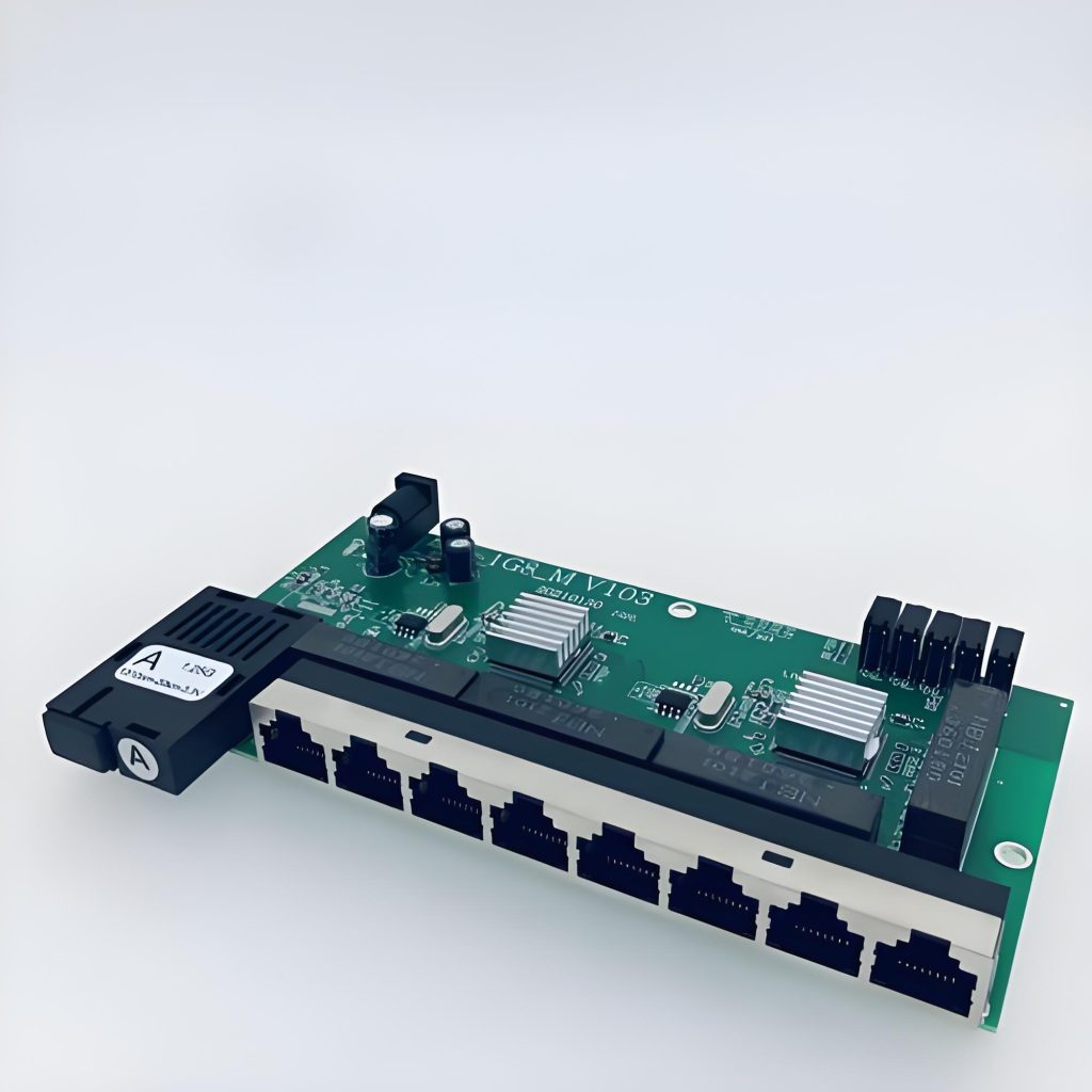
Industriekontrollen
- SPS-speicherprogrammierbare Steuerungen
- Energieverwaltungsmodule
- Instrumentierungsplatinen
- Steuerplatinen für Motorantriebe
Kfz -Elektronik (Nicht sicherheitskritisch)
- Infotainmentsysteme im Fahrzeug
- Karosseriesteuermodule
- Sensorschnittstellenkarten
Qualitätssicherung und Einhaltung von Standards
Anwendbare Standards
Das OSP-Antioxidans-PCB-Produkt von UGPCB hält sich strikt an diese internationalen Standards:
| Standard | Titel | Umfang |
|---|---|---|
| IPC-4555 | Leistungsspezifikation für organische Hochtemperatur-Lötschutzmittel (OSP) für Leiterplatten | Anforderungen und Tests des OSP-Prozesses |
| IPC-6012E | Qualifikations- und Leistungsspezifikation für starre Leiterplatten | Qualität und Leistung des fertigen Boards |
| IPC-4101/21 | Spezifikation für glasfaserverstärktes Epoxidlaminat | Technische Anforderungen an das FR-4-Substrat |
| IPC-TM-650 | Handbuch zu Testmethoden | Verschiedene Leistungstestmethoden |
| UL 94 V-0 | Entflammbarkeit von Kunststoffmaterialien | Flammhemmende Sicherheit des Untergrundes |
| RoHS 2.0 | Beschränkung gefährlicher Stoffe | Umweltkonformität |
Wichtige Qualitätsindikatoren
Gemäß IPC-Anforderungen, Zu den wichtigsten Qualitätskennzahlen gehören::
- OSP-Foliendicke: 0.2–0,5μm, Gleichmäßigkeitstoleranz ≤ ±0,1μm
- Haftung: ≥4B (IPC-TM-650 2.4.29 Kreuzschnitttest)
- Lotausbreitungsverhältnis: ≥80 % (IPC-TM-650 2.4.1)
- Oxidationsschutzzeitraum: ≥6 Monate (Umgebungsbedingungen)
- Entflammbarkeitsbewertung: UL 94 V-0
Warum sollten Sie sich für UGPCB für antioxidative OSP-Leiterplatten entscheiden??
Präzisionsfertigungskapazitäten
- 0.15mm Mindestspurbreite / 0.20mm Mindestabstand
- 0.45mm minimale fertige Lochgröße
- 1.6mm Standardplattenstärke mit hervorragender Kompatibilität
Zuverlässige OSP-Prozesssteuerung
- Strikte Einhaltung von IPC-4555 für Filmdicke und -qualität
- Vollständige Rückverfolgbarkeit während des gesamten Herstellungsprozesses
- Lötbarkeitsprüfung und Schichtdickenprobenahme für jede Charge
Schnelle Lieferung
- Standardvorlaufzeit: 7–10 Werktage
- Unterstützt sowohl die Bemusterung von Prototypen als auch die Massenproduktion
Umfassender technischer Support
- Kostenlose DFM-Designprüfung
- Professionelles Engineering-Team zur Produktauswahlberatung
Holen Sie sich noch heute ein Angebot ein
UGPCB liefert hochwertige, antioxidative OSP-Leiterplattenlösungen. Ob Sie brauchenPrototypenbemusterung oderMassenproduktion, Wir bieten professionellen technischen Support und wettbewerbsfähige Preise.
📞 So erhalten Sie ein Angebot:
- Senden Sie Ihre Gerber-Dateien und Stücklisten
- Unser Engineering-Team antwortet mit einer maßgeschneiderten Lösung und einem Angebot24 Std.
- Kostenloser DFM-Check, um sicherzustellen, dass Ihr Design beim ersten Mal erfolgreich ist
Erklärung zur Datenquelle: Die in diesem Dokument genannten technischen Daten und Standardanforderungen stammen hauptsächlich aus IPC (Verband zur Verbindung der Elektronikindustrie) Standards einschließlich IPC-4555 “Leistungsspezifikation für organische Hochtemperatur-Lötschutzmittel (OSP) für Leiterplatten,” IPC-6012E “Qualifikations- und Leistungsspezifikation für starre Leiterplatten,” IPC-4101/21 “Spezifikation für glasfaserverstärktes Epoxidlaminat,” IPC-TM-650 “Handbuch zu Testmethoden,” und UL 94 “Norm für Tests zur Entflammbarkeit von Kunststoffmaterialien für Teile in Geräten und Geräten.” Einige Prozessparameter verweisen auf öffentlich verfügbare technische Daten führender Leiterplattenhersteller. Alle Daten wurden auf ihre Richtigkeit überprüft.













