

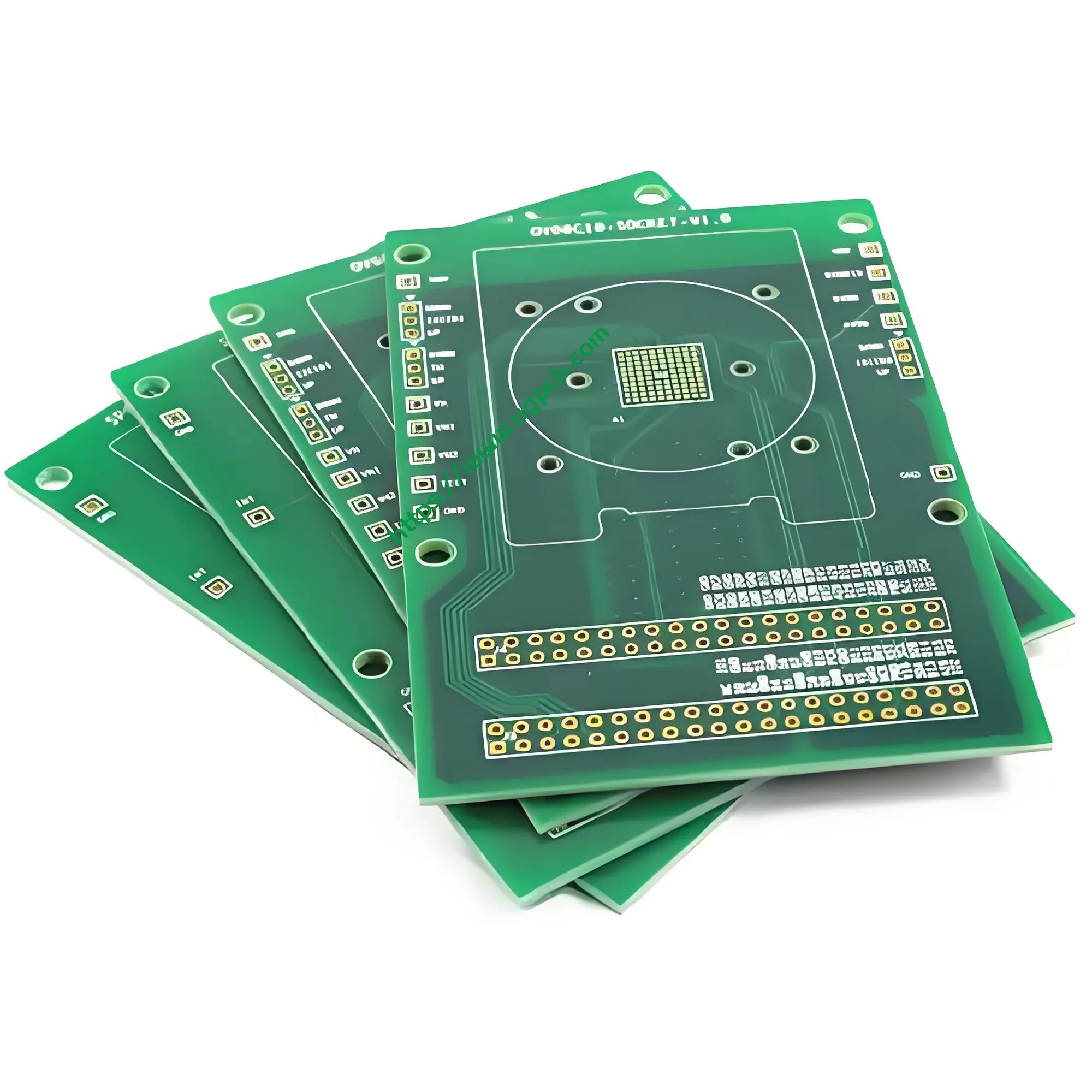
1. Produktübersicht: Was ist eine Leiterplatte für einen kabellosen Staubsauger??
Eine Leiterplatte für einen kabellosen Staubsauger (Leiterplatte) ist die zentrale elektronische Komponente, die für die Motorantriebssteuerung verantwortlich ist, Energieverwaltung, Benutzerinteraktion, und Sicherheitsschutz in einem kabellosen Staubsauger. In einfachen Worten, Es dient als „Gehirn“ und „Nervenzentrum“ des Geräts. Es empfängt Tastenbefehle, Steuert die Geschwindigkeit des bürstenlosen Motors, verwaltet das Laden und Entladen der Batterie, überwacht den Betriebszustand, und implementiert mehrere Sicherheitsmaßnahmen.
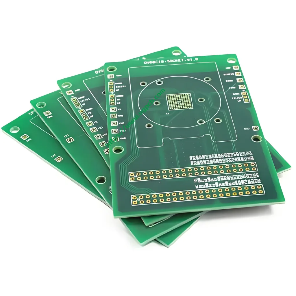
UGPCB stellt diese Leiterplatte für kabellose Staubsauger vor – a 2-Schicht starre Leiterplatte Speziell für tragbare Reinigungsgeräte entwickelt. Es nutzt FR-4-Glas-Epoxid-kupferbeschichtetes Laminat als Grundmaterial. Die Plattenstärke beträgt 1,0 mm, und die Abmessungen sind 86.37 × 72,6 mm. Diese kompakte Größe passt perfekt in die engen Innenräume von Hand- und Stabstaubsaugern.
Gemäß IPC-6012F Qualifikations- und Leistungsspezifikation für starre Leiterplatten, Dieses Produkt fällt unter die starre doppelseitige Leiterplatte (mit durchkontaktierten Löchern) Kategorie. Als wichtiger Bestandteil des One-Stop-Angebots von UGPCB Leiterplatte Lösungen, Dieses Produkt erfüllt die internationalen IPC-Standards vom Design über die Herstellung bis hin zur Qualitätskontrolle. Es bietet Staubsaugerherstellern eine hohe Zuverlässigkeit, kostengünstig Leiterplatte Lösung.
2. Produktklassifizierung: Wissenschaftliche Positionierung und Branchenkategorisierung
Gemäß IPC-6012F und Standardplatine Branchenklassifizierungssysteme, Dieses Produkt kann wissenschaftlich wie folgt kategorisiert werden:
| Klassifizierungsdimension | Kategorie |
|---|---|
| Durch Struktur | Starre doppelseitige Leiterplatte (mit durchkontaktierten Löchern) |
| Nach Basismaterial | FR-4-Epoxidharz-Glaslaminat mit Kupferbeschichtung (konform mit IPC-4101) |
| Für Schichtzahl | 2-Schichtplatte (Doppelseitige PCB) |
| Nach Oberflächenbeschaffenheit | Bleifreies HASL (Heißluftlötes Leveling) |
| Nach Brennbarkeitsbewertung | UL 94 V-0 |
| Durch Anwendung | Unterhaltungselektronik / Steuerplatine für Kleingeräte (Staubsauger PCBA) |
Innerhalb der Staubsauger-Elektronikindustrie, Dieses Produkt gehört zurMotorantrieb und Steuerung PCBA Kategorie. Zusammen mit der Hauptsteuerplatine und der Energieverwaltungsplatine, Es bildet die drei Kernschaltkreismodule eines kabellosen Staubsaugers.
3. Wichtige technische Parameter
3.1 Grundmaterial und Plattenstärke
- Grundmaterial: FR-4 (glasfaserverstärktes, mit Epoxidharz beschichtetes Laminat)
- Brettdicke: 1.0mm
FR-4 ist das am häufigsten verwendete starre Substrat in der Leiterplattenindustrie. Für IPC-4101, FR-4 bietet eine hervorragende elektrische Isolierung, mechanische Stärke, und Wärmewiderstand. Standard FR-4 hat eine Glasübergangstemperatur (Tg) von 130–140°C. Für IPC-6012, Der Toleranzbereich für eine Plattendicke von 1,0 mm beträgt ±0,1 mm.
3.2 Anzahl und Abmessungen der Ebenen
- Schichtzahl: 2 Schichten (Doppelseitige Brett)
- Abmessungen: 86.37 × 72.6 mm
Die zweischichtige Struktur kontrolliert effektiv die Herstellungskosten und liefert gleichzeitig eine solide elektrische Leistung. Dies macht es zur Mainstream-Wahl für kabellose Staubsauger-Steuerplatinen. Der Kompakte 86.37 Die Abmessungen von × 72,6 mm sind für den begrenzten Platz im Inneren von Staubsaugern optimiert.
3.3 Leiterbahnbreite/-abstand und Mindestlochgröße
- Mindestlochgröße: 0.45mm
- Spurenbreite/Abstand: 0.45mm / 0.391mm
Gemäß IPC-2221CAllgemeiner Standard für Leiterplattendesign, Bei der Gestaltung der Leiterbahnbreite und -abstände muss die elektrische Leistung berücksichtigt werden, Strombelastbarkeit, und Fertigungskapazität. Die minimale Lochgröße von 0,45 mm unterstützt das zuverlässige Löten herkömmlicher DIP-Komponenten und Durchgangslochteile.
Für Strombelastbarkeit, die branchenübliche FormelI = k·ΔT^0,44·A^0,725 (wobei A die Querschnittsfläche der Spur ist) zeigt das mit 1 Unze Kupfer, a 0,45mm (ca. 18Mil) Die Leiterbahn kann etwa 1,8–2,0 A tragen. Die Leiterplatte des kabellosen Staubsaugers nutzt diese Leiterbahnbreite für Motorantriebssignale und Steuersignale, Gewährleistung eines langfristig stabilen Betriebs.
3.4 Dicke der Kupferfolie
- Dicke der Kupferfolie: 1/1 OZ (1 Unze auf beiden Außenschichten)
1Unze Kupferfolie (ca. 35μm) ist die Standardkonfiguration für Leiterplatten der Unterhaltungselektronik. Es bietet ein hervorragendes Gleichgewicht zwischen der Strombelastbarkeit, Wärmeleitfähigkeit, und Kosten.
3.5 Oberflächenbeschaffung
- Oberflächenbeschaffung: Bleifreies HASL (Heißluftlötes Leveling)
HASL ist ein ausgereiftes und wirtschaftliches PCB-Oberflächenfinish. Bleifreies HASL erfüllt die RoHS-Umweltanforderungen. Gemäß IPC-Standards, Bleifreies HASL hat typischerweise eine Zinnschichtdicke von 1–40 μm, mit herkömmlichen Prozessen, die auf 5–25 μm gesteuert werden. Diese Oberfläche bietet eine hervorragende Lötbarkeit (Benetzbarkeit) und eine gute Lagerfähigkeit von bis zu 12 Monate.
3.6 Lötmaske und Legende
- Farbe der Lötmaske: Grüne Tinte
- Legendenfarbe: Weiß
Grüne Lötstopplacke sind in der Branche die beliebteste Wahl. Es bietet hervorragenden Isolationsschutz und hohen Kontrast AOI (Automatisierte optische Inspektion). Weiße Legenden sind klar und leicht zu lesen, Dies erleichtert die Platzierung der Komponenten und die zukünftige Wartung.
4. Entwurfsrichtlinien: Gemäß IPC-2221C-Standards
Eine gut gestaltete Leiterplatte für einen kabellosen Staubsauger muss diesen Grundprinzipien folgen (gemäß IPC-2221C):
4.1 Elektrisches Leistungsdesign
- Breite der Leistungsspur: Berechnen Sie mit der Formel I = k·ΔT^0,44·A^0,725 um sicherzustellen, dass der Temperaturanstieg bei maximalem Betriebsstrom unter 10 °C bleibt.
- Signalintegrität: Verwenden Sie für Steuersignale eine Leiterbahnbreite von 0,45 mm, um eine vollständige Übertragung von PWM-Geschwindigkeitssteuersignalen und Sensorsignalen zu gewährleisten.
- Erdungsdesign: Verwenden Sie Einzelpunkt-Erdungs- oder Split-Erdungsstrategien, um Störungen des Regelkreises durch die Stromschleife zu verhindern.
4.2 Wärmemanagement-Design
Kabellose Staubsauger erzeugen während des Betriebs erhebliche Wärme durch MOSFETs. Der PCB-Design muss dies beheben:
- Platzierung thermischer Via-Arrays unter Leistungsgeräten.
- Erweitern Sie Hochstromleiterbahnen oder fügen Sie freiliegendes Kupfer hinzu, um die Wärmeableitung zu verbessern.
- Verwendung einer Plattendicke von 1,0 mm, um Wärmeleitfähigkeit und mechanische Festigkeit auszugleichen.
4.3 Mechanisches Strukturdesign
Der 86.37 Die Abmessungen von × 72,6 mm müssen genau zum Staubsaugergehäuse passen. Die Positionen der Befestigungslöcher und der Anschlüsse müssen den strukturellen Designanforderungen entsprechen. Die Mindestlochgröße von 0,45 mm unterstützt das Durchstecklöten verschiedener DIP-Komponenten und Steckverbinder.
5. Arbeitsprinzip
Die Leiterplatte des kabellosen Staubsaugers durchläuft die folgenden Kernprozesse:
① Stromeingang und -management: Der Lithium-Akku (typischerweise 21,6 V oder 25,2 V) durchläuft den Stromverwaltungsschaltkreis auf der Platine. Dadurch werden stabile Spannungen für den Hauptsteuerchip und die Treiberschaltkreise bereitgestellt.
② Berechnung des Hauptsteuerchips: Das MCU (Mikrocontroller) auf der Platine empfängt Tastenbefehle. Es berechnet und gibt dreiphasige Antriebssignale mithilfe von FOC aus (Feldorientierte Steuerung) oder Rechteck-Steueralgorithmen.
③ Motorantrieb: Die Antriebssignale werden durch MOSFET-Leistungsgeräte verstärkt. Diese Signale treiben dann den bürstenlosen Gleichstrommotor an (BLDC) mit hoher Geschwindigkeit rotieren lassen, Erzeugt den zum Absaugen benötigten Luftstrom.
④ Feedback und Schutz: Die Platine überwacht kontinuierlich den Motorstrom, Batteriespannung, Temperatur, und andere Parameter. Wenn abnormale Bedingungen wie Überstrom erkannt werden, Übertemperatur, Unterspannung, oder Rotorsperre, es führt sofort Schutzmaßnahmen aus.
6. Materialien verwendet
| Komponente | Material | Beschreibung |
|---|---|---|
| Substrat | FR-4 Glasepoxidharz | Konform mit IPC-4101 |
| Leitfähige Schicht | Elektrolytische Kupferfolie (1oz) | 1Unzen auf beiden Außenschichten |
| Lötmaske | Grüne, fotografisch bebilderbare Tinte | Isolationsschutz, Oxidationsbeständigkeit |
| Oberflächenbeschaffung | Bleifreie HASL-Legierung | ROHS -konform |
| Legendentinte | Weiße Epoxidtinte | Hoher Kontrast, hitzebeständig |
FR-4-Substrat trägt ein UL 94 V-0 Entflammbarkeitsbewertung. Im vertikalen Brenntest, Die Flamme erlischt im Inneren 10 Sekunden nach dem Entfernen, ohne brennende Tropfen. Diese Funktion ist für hohe Leistung von entscheidender Bedeutung, batteriebetriebene Geräte wie kabellose Staubsauger. Es reduziert die Brandgefahr durch Stromkreisfehler erheblich.
7. Leistungsspezifikationen
7.1 Elektrische Leistung
| Parameter | Spezifikation | Referenzstandard |
|---|---|---|
| Isolationswiderstand | ≥10^6 MΩ | IPC-6012F |
| Dielektrische Spannungsfestigkeit | Bis zu 500V (designabhängig) | IPC-2221C |
| Leitungswiderstand | ≤50mΩ (typisch) | IPC-6012F |
| Charakteristische Impedanz | Auf Wunsch steuerbar (50Ω/90Ω/100Ω) | IPC-2221C |
7.2 Wärmeleistung
| Parameter | Spezifikation | Referenzstandard |
|---|---|---|
| Glasübergangstemperatur (Tg) | ≥135°C (DSC-Methode) | IPC-TM-650 2.4.25 |
| Löthitzebeständigkeit | 288°C / 10S, Keine Delaminierung | IPC-4101 |
| Z-Achse CTE (CTEz) | ≤65 ppm/°C (50–260°C) | IPC-4101 |
7.3 Mechanische Leistung
| Parameter | Spezifikation | Referenzstandard |
|---|---|---|
| Toleranz der Plattendicke | ±0,1 mm | IPC-6012 |
| Lochgrößentoleranz | ±0,05 mm | IPC-6012F |
| Entflammbarkeitsbewertung | UL 94 V-0 | UL 94 |
7.4 Zuverlässigkeit
- Lötbarkeitstest: Konform mit IPC-J-STD-003
- Alterungstest: 500 Stunden unter Double-85-Bedingungen (85°C / 85%RH) ohne Auffälligkeiten
8. Strukturelle Merkmale
8.1 2-Vorteile von Layer-Boards
Die oberste Schicht trägt die Hauptkomponenten und Signalspuren. Die untere Schicht verwaltet Hilfskomponenten und Erdungs-/Stromkupfergüsse. Das 2-Lagen-Design erreicht diesbeste Kosten Undhöchste Zuverlässigkeit Balance für kabellose Staubsauger-Steuerungsfunktionen.
8.2 Durchkontaktiertes Loch (PTH) Verfahren
Bei allen Durchgangslöchern kommt das Durchkontaktierungsverfahren zum Einsatz. Dies gewährleistet eine zuverlässige Verbindung zwischen Ober- und Unterschicht. Es bietet außerdem eine solide mechanische Unterstützung und elektrische Verbindung für DIP-Komponenten.
8.3 Lötmaskenbrückenprozess
Die grüne Lötmaske bildet Brücken zwischen benachbarten Pads. Dies verhindert Lötkurzschlüsse und verbessert die SMT-Bestückungsausbeute.
9. Ablauf des Herstellungsprozesses
UGPCB befolgt strikt die IPC-6012F-Standards, um jeden Produktionsschritt zu kontrollieren:
① Wareneingangskontrolle →② Erstellung innerer Schaltkreise (für 2-Schicht-Platten, Dies ist direkt die äußere Schicht) →③ Laminierung (Gilt nicht für 2-Schicht-Platten) →④ Bohren (Mindestlochgröße 0,45 mm) →⑤ Stromlose Kupferabscheidung / Plattenbeschichtung →⑥ Außenschichtschaltung →⑦ Musterbeschichtung →⑧ Radierung →⑨ Lötmaske (grüne Tinte) →⑩ Oberflächenbeschaffenheit (bleifreies HASL) →⑪ Legende (weiße Zeichen) →⑫ Profilrouting (86.37 × 72,6 mm) →⑬ Elektrischer Test →⑭ Endkontrolle (für IPC-A-600) →⑮ Verpackung und Versand
Jede Charge wird durchlaufenFlying-Probe-Tests oderspezielle Vorrichtungstests zu gewährleisten 100% Keine Unterbrechungen oder Kurzschlüsse.
10. Anwendungsszenarien
10.1 Primäranwendungen
- Handstaubsauger ohne Kabel: Motorantrieb und -steuerung auf engstem Raum
- Akku-Staubsauger im Stielstil: Batteriemanagement und bürstenloser Motorantrieb
- Roboterstaubsauger: Navigationssteuerung und Motorantrieb
- Autostaubsauger: 12V/24V-Stromanpassung und -steuerung
- Intelligente Reinigungsgeräte: IoT-Konnektivität und intelligente Steuerung
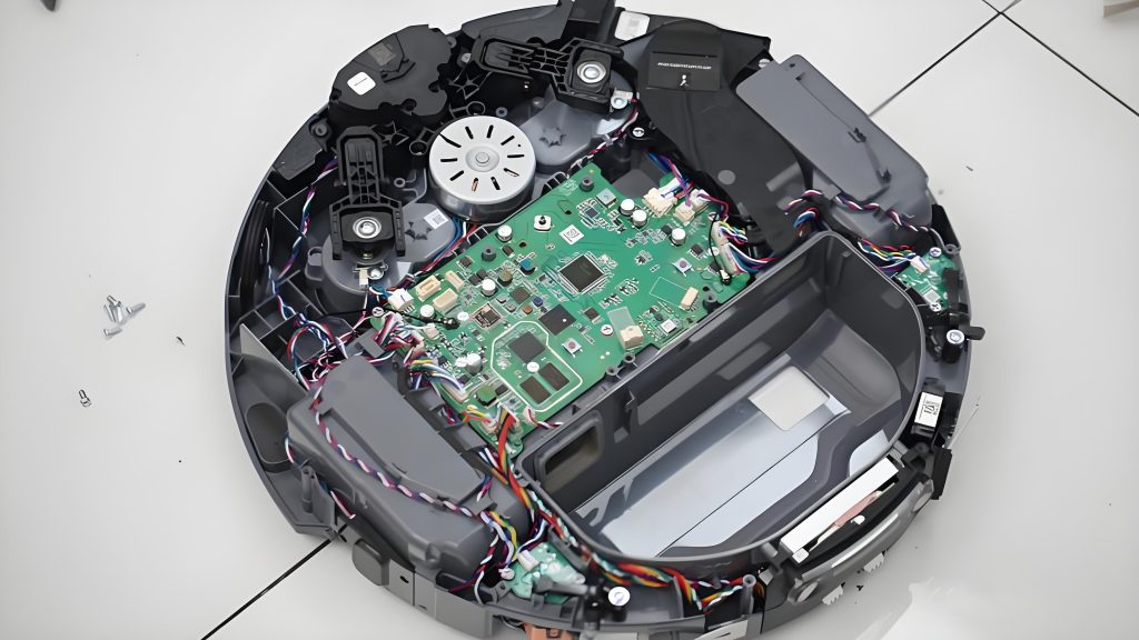
10.2 Beispiele für Endprodukte
Diese Leiterplatte kann häufig in Steuerplatinen und Treiberplatinen für kabellose Staubsauger und ähnliche Reinigungsgeräte von Marken wie Xiaomi verwendet werden, Dyson, Tineco, und Leifheit.
11. Warum sollten Sie sich für die kabellose Staubsaugerplatine von UGPCB entscheiden??
✅Einhaltung internationaler Standards: Design, Herstellung, und Inspektion entsprechen vollständig IPC-6012F, IPC-A-600, IPC-2221C, und andere internationale Standards
✅UL 94V-0 Brandschutz: FR-4-Substrat erreicht die höchste vertikale Brennleistung, Gewährleistung der Gerätesicherheit

✅Bleifreier, umweltfreundlicher Prozess: Die bleifreie HASL-Oberflächenveredelung entspricht den Umweltrichtlinien RoHS und REACH
✅Bewährte Fertigungsfähigkeit: UGPCB bietet Dienstleistungen aus einer Hand vom PCB-Design und der PCB-Herstellung bis zur PCBA-Montage
✅Strenge Qualitätskontrolle: Sichtprüfung gemäß IPC-A-600 und 100% Elektrische Tests stellen die Versandqualität sicher
✅Kompakte, optimierte Abmessungen: Der 86.37 Die Größe von × 72,6 mm passt perfekt in den Innenraum verschiedener kabelloser Staubsauger
12. Holen Sie sich noch heute ein Angebot und Muster
UGPCB steht für höchste Präzision, hochzuverlässige PCB- und PCBA-Lösungen für Elektronikhersteller weltweit. Ob Sie brauchen blanke Leiterplatten, komplett montierte PCBA, oder Dienstleistungen aus einer Hand vom Design bis zur Massenproduktion, UGPCB verfügt über das Fachwissen, um Sie zu unterstützen.
📧Kontaktieren Sie UGPCB noch heute für ein individuelles Angebot →
- Webseite: www.ugpcb.com
- Kundenspezifische Designänderungen und -optimierungen möglich
- Kostenloses DFM (Design für die Herstellung) Rezension
- Schneller Prototypenbau und Serienproduktion sind möglich
Datenquellendeklaration
Die in diesem Artikel zitierten technischen Standards und Daten stammen von den folgenden maßgeblichen Organisationen:
- IPC (Verband zur Verbindung der Elektronikindustrie): IPC-6012F Qualifikations- und Leistungsspezifikation für starre Leiterplatten, IPC-A-600 Akzeptanz von Leiterplatten, IPC-2221C Allgemeiner Standard für Leiterplattendesign, IPC-4101 Spezifikation für Basismaterialien für starre und mehrschichtige Leiterplatten, IPC-TM-650 Handbuch zu Testmethoden
- UL (Underwriters Laboratories): UL 94 Norm zur Sicherheit und Entflammbarkeit von Kunststoffmaterialien für Teile in Geräten und Geräten – V-0 Bewertung
- Industriestandard-Engineering-Formel: Formel für die Strombelastbarkeit der Leiterplatte I = k·ΔT^0,44·A^0,725













