
La révolution du matériau silencieux remodelant l'électronique
Intel 2024 Début mondial du verre emballage de substrat La technologie a fait exploser un changement sismique dans la fabrication de semi-conducteurs. Au 2025 Summit de l'industrie Suzhou TGV, Leaders techniques d'Intel, Tsmc, Et Samsung est d'accord: “Les substrats en verre entraîneront des emballages semi-conducteurs dans une «ère transparente,’ avec la pénétration du marché dépassant 50% dans les cinq ans.” Cette analyse explore la justification technologique, transformation de la chaîne industrielle, et implications pour PCB industries.
1. Supériorité technique: Pourquoi les substrats de verre redéfinissent l'emballage
1.1 Dominance des propriétés physiques
L'analyse comparative révèle des substrats en verre’ Avantages écrasants :
| Paramètre | Substrats organiques | Interposants en silicium | Substrats de verre |
|---|---|---|---|
| Constante diélectrique | 4.2-4.8 | 11.9 | 3.9 |
| Perte tangente | 0.02-0.04 | 0.001-0.01 | 0.0001-0.001 |
| CTE (ppm/°C) | 16-18 | 2.6 | 3.2-7.5 (réglable) |
| Conductivité thermique | 0.2-0.3 | 150 | 1.1 |
| Rugosité de surface | 0.5-1.0 µm | 0.05 µm | <0.01 µm |
(Source: Livre blanc technique Intel, Corning Materials Lab)
Analyse de l'équation de la perte de signal
Atténuation (un) est défini comme:

Avec ε’≈3.9 et ε”≈0,001 pour les substrats en verre, haute fréquence (100GHz) Les pertes réduisent de 67% Versus substrats organiques (E'4.5, e”≈0,03).
1.2 Amélioration de la densité exponentielle
Le GB 200 GB de Nvidia démontre 50%+ Augmentation du nombre de matrices à l'aide de substrats en verre, atteindre une densité de câblage de 5 μm / 5 μm à travers:
-
Planéité au niveau atomique (<0.01μm de rugosité)
-
Correspondance CTE accordable (3ppm/°C)
-
Stabilité mécanique (700Warpage de panneau de 700 mm de 700 mm <50µm)
2. Traiter les innovations: Industrialiser la technologie TGV
2.1 Percèdes de fabrication de VIA à travers
La modification laser de Titanrise Tech atteint 8,000 vias / sec à ± 5 μm de précision (3un), 160× plus rapide que les méthodes conventionnelles. Étapes clés:
-
Modification laser picoseconde: Crée des zones modifiées à l'échelle micron
-
Gravure HF: Réaliser 100:1 rapport d'aspect
-
Métallisation: Pulvérisation du PVD + électroplaste (>15Adhésion MPA)
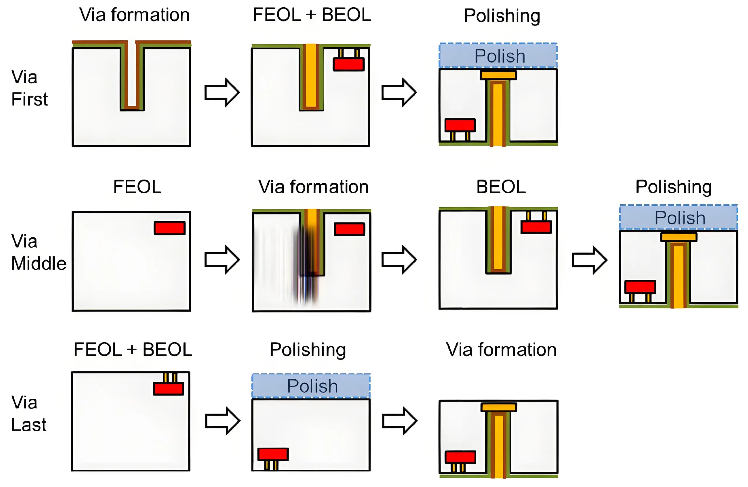
2.2 Avancées de métallisation
Quatre routes techniques abordent l'adhérence en verre:
-
Sans électronique avec + Micro-gravure (Solutions AKM)
-
Pâte de nano-ag + LT Strons (Brevet wintech)
-
Greffe de plasma (Technologie IME-CAS)
-
PVD TI / avec pile (Titanrise Standard)
Parmi eux, UGPCB a investi massivement dans l'introduction de l'équipement DEP600, qui adopte la technologie de pulvérisation des rapports d'aspect élevé, réalisation 95% couverture 10:1 profils de trous, avec une résistivité métallique de moins de 2.5 μω · cm, atteindre un niveau de tête international.
3. Paysage de l'industrie: La concurrence mondiale s'intensifie
3.1 Projections de croissance du marché
Prismark prévoit une expansion explosive:
-
2025: $916M (Substrats TGV)
-
2030: $4.2B (Applications complètes)
-
2035: $11.3B (écosystème entier)
3.2 Race technologique géopolitique
-
USA: Normes Intel + Dominance de l'offre de Corning
-
Corée: Samsung “Alliance de verre” + Les piles de 9 couches de SKC
-
Chine: Production de masse Wintech / AKM + Jfe 2026 localisation
4. Défis & Solutions: Haies de commercialisation
4.1 Pathways de réduction des coûts
La prime de coût 3-5 × actuelle vs les substrats traditionnels chuteront à travers:
-
85% grand panneau (>2m²) utilisation
-
90% Réduction des coûts de forage au laser
-
Amélioration des rendements de métallisation (60%→ 92%)
4.2 Certification de fiabilité
Nouvelles normes requises:
-
Cyclisme thermique (-55° C - 250 ° C, 1,000 cycles)
-
Em Lifetime (MTTF >10⁷ Heures @ JEP154)
-
Stabilité à haute fréquence (<0.5db / cm @ 100GHz)
5. Implications de l'industrie des PCB: Menace vs opportunité
5.1 Perturbation du marché
-
30% HDI /substrat risque de remplacement
-
Hybride (verre + résine) Opportunités de substrat
5.2 Synergies technologiques
-
Adoption de forage laser picoseconde
-
Amélioré par le PVD IDH précision trace
-
Inspection optique <0.1Résolution μm
Conclusion: Substrats transparents, Avenir opaque
La Chine mène maintenant les secteurs critiques de TGV (équipement, essai, matériels). Comme le note Pat Gelsinger d'Intel: “L'innovation matérielle devient la nouvelle loi de Moore à des échelles atomiques.” Cette révolution axée sur le verre peut débloquer la deuxième courbe de croissance de Semiconductor.
