
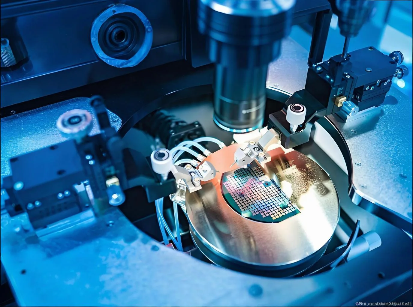
Chaque progression microscopique dans la technologie d'emballage remodeler les limites physiques de l'électronique.
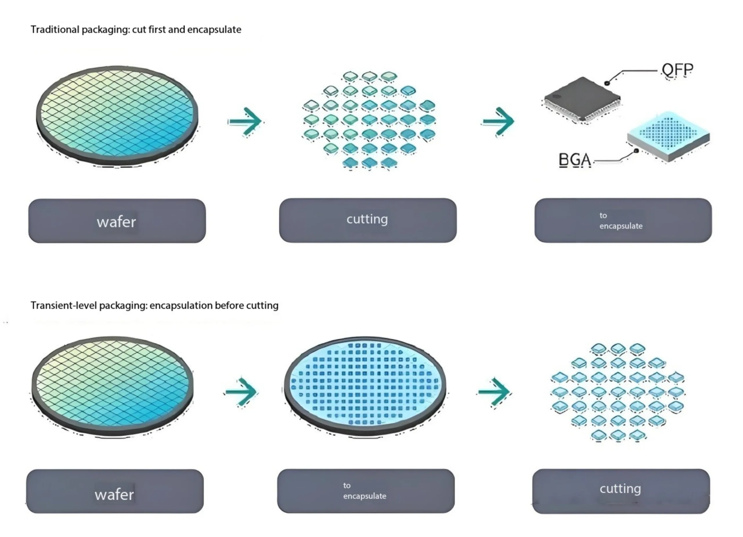
Dans la semaine dernière Évolution de l'emballage des puces: De DIP à X2SON - comment la miniaturisation a remodelé l'électronique, Nous avons exploré l'ère de l'emballage à travers un trou à travers (TREMPER) et comment les appareils de montage en surface (AMADOUER, Observation, FILS) miniaturisation de dispositif initié. Alors que ces technologies ont posé des fondations d'emballage modernes, le Révolution de la miniaturisation continue. Aujourd'hui, Nous examinons des packages de densité plus élevée - du quad-plate à la CSP au niveau de la plaquette - et de leur impact sur Conception de circuits imprimés limites.
Packages quadruples: L'équilibre de la densité spatiale
Packages quadruples (CFP, PLCC / QFJ, QFN) représentent une évolution critique vers une densité d'E / S plus élevée en utilisant les quatre bords de package.
CFP: Le pionnier de la densité de la goéle
CFP (Ensemble quadruple) Caractéristiques emblématiques “mouette” (En forme de L) conduit s'étendant de tous les côtés. C'est tangage d'épingle (0.4mm / 0,5 mm / 0,65 mm) dicter Routage de PCB Densité et précision de soudage.
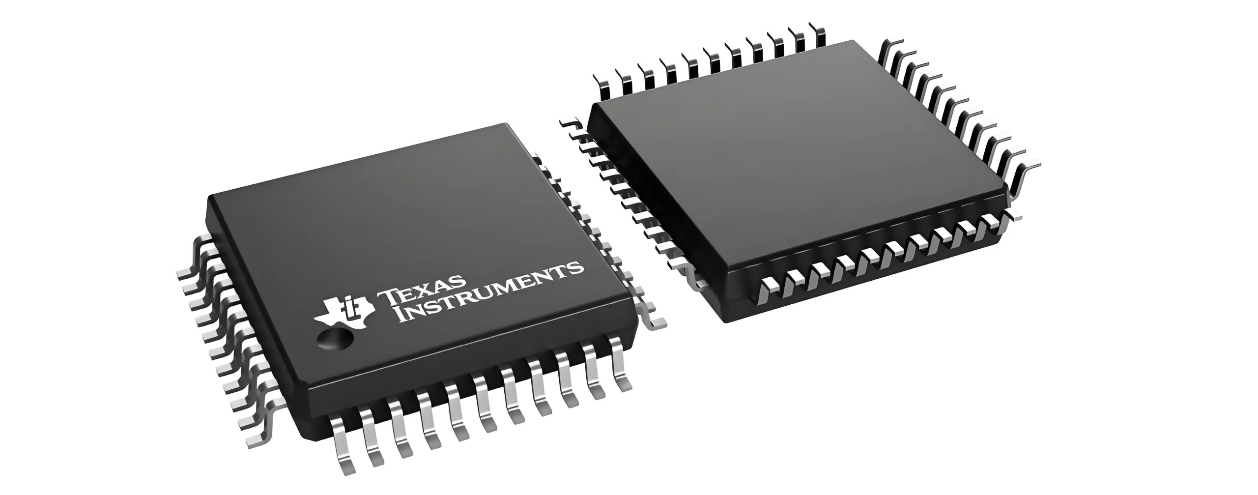
Variants QFP:
-
Taille / épaisseur: LQFP (À profil discret), Tqfp (Mince), Vqfp (Très mince)
-
Matériel: Pqfp (Plastique), MQFP (Métal)
-
Thermique amélioré: HQFP, Hlqfp, Htqfp, Hvqfp
-
Protection: Bqfp (Les coussinets exceptionnels - les coussins empêchent les fils pliés)
La gestion thermique est critique. La formule de résistance thermique à la jonction à ambiance θja = (Tj - ta)/P. (où TJ= température de la jonction, Parement= température ambiante, P.= puissance) régit la conception de dissipation de chaleur.
PLCC / QFJ: Stabilité à travers j-leads
PLCC (Support de puce en plastique) ou qfj (Quad plate j-lede) Utilise des fils en J en forme de J pour une stabilité mécanique contre les vibrations / contrainte thermique.
Avantage de normalisation: La forte compatibilité de PLCC / QFJ avec les prises de test universelles rationalise les tests de production. Bien que QFJ soit techniquement précis, “PLCC” reste préfère de l'industrie.
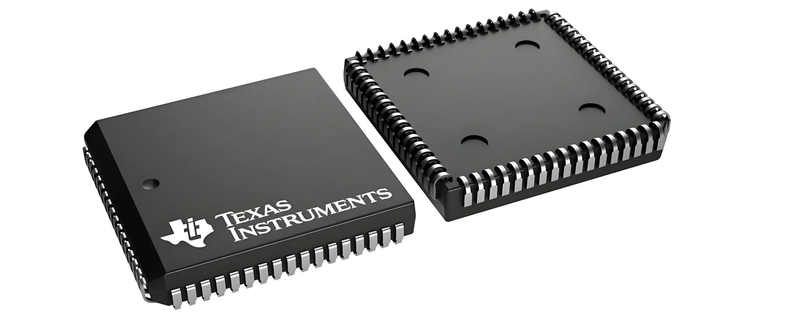
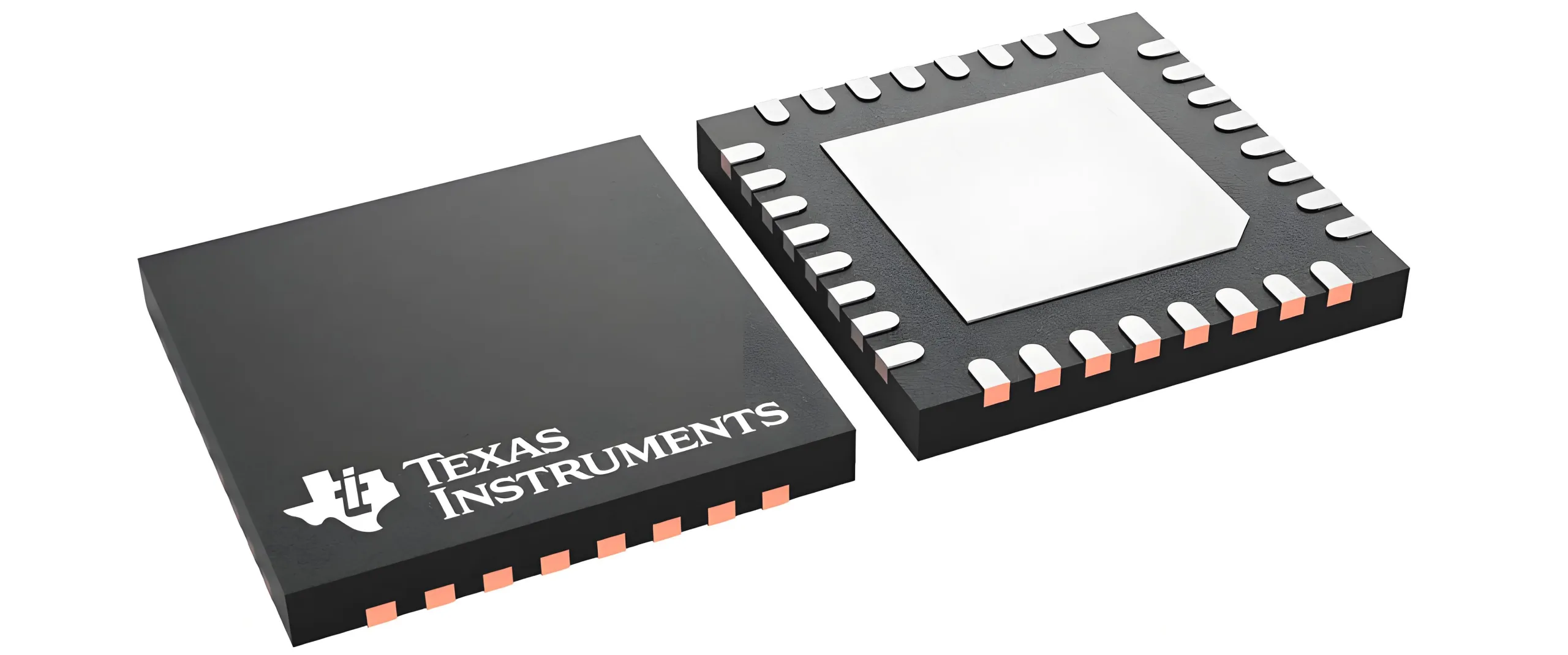
QFN: Percée de miniaturisation sans plomb
QFN (Quad plat sans plaidoirie) élimine les pistes externes, Connexion via:
-
Coussin exposé (EP): Chemin thermique direct vers PCB cuivre
-
Flancs mouillables: Tampons de soudable paroi latérale
Avantages clés:
-
Ultra-compact: 40% plus petit que QFP
-
Supériorité électrique: Des chemins plus courts réduisent l'inductance parasite (L ≈ μ · l / w)
-
Efficacité thermique: Inférieur θja vs. QFP de même taille
Évolution d'épaisseur: Lqfn → uqfn → vqfn → wqfn → x1qfn → x2qfn. LCC (LPCC / LCCC) est sa variante en céramique / plastique sans plomb.
Forfaits: Révolutionner les limites de densité
Lorsque le quad-plate atteint les limites d'E / S, forfaits (LGA, BGA) Activer la densité d'interconnexion 2D.
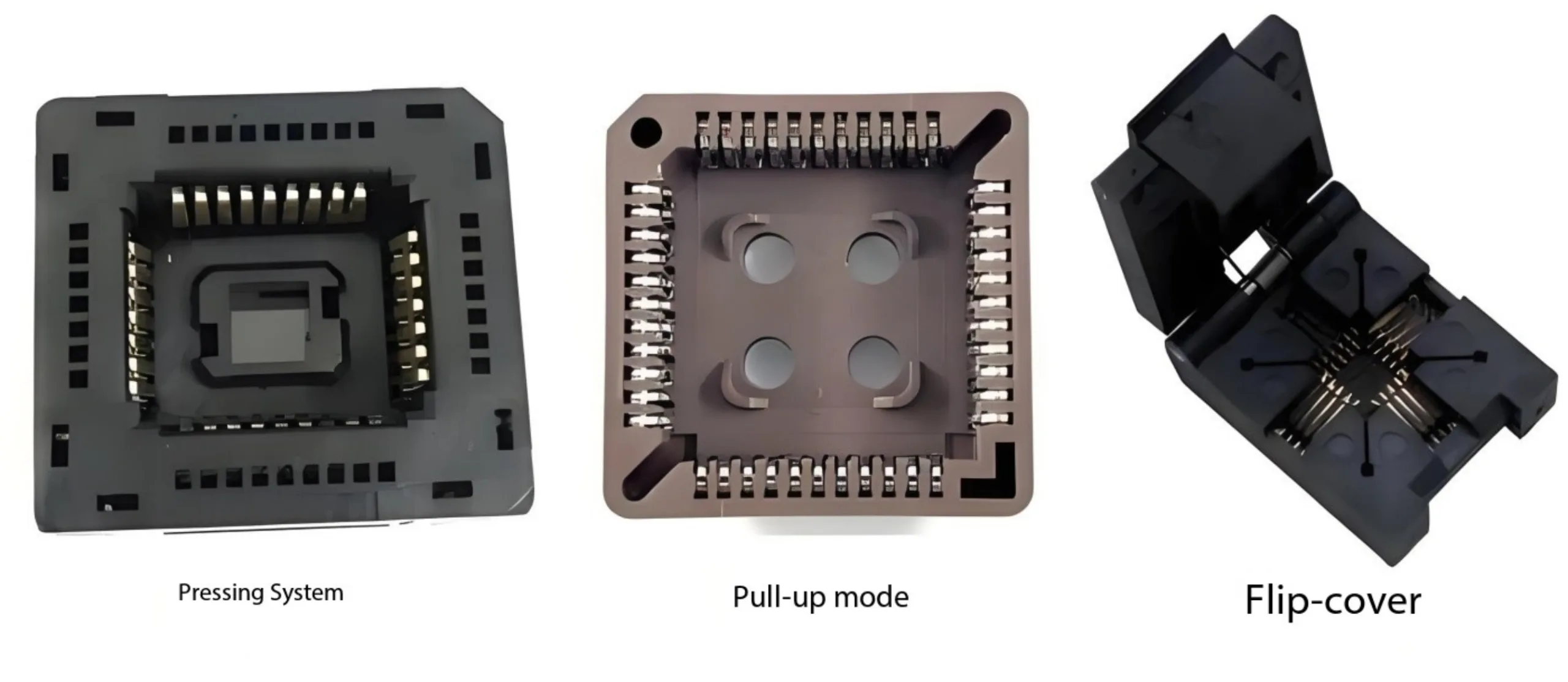
LGA: Connexion élastique de précision
LGA (Tableau de la grille terrestre) utilise des contacts métalliques alignés précisément (par ex., LGA775: 775 contacts) s'accoupler avec des épingles à douille.
Valeur fondamentale:
-
Sottiabilité: Mises à niveau / maintenance du processeur
-
Inductance faible: Chemins de signaux courts
-
Haute fiabilité: Idéal pour les processeurs (Intel / AMD)
Limitation: Coût / taille de socket élevé Favors BGA dans les appareils compacts. Note: Les LGA peuvent être soudés directs.
BGA: La domination de la boule de soudure
BGA (Tableau de grille à billes) se connecte via une matrice à billes de soudure. Pas de balle (0.3–1,0 mm; <0.2MM pour FBGA) est critique.
Avantages transformateurs:
-
Densité élevée: >1,000 Je / nous (contre. QFP ~ 300)
-
Économie d'espace: 30%+ réduction de la zone vs. CFP
-
Électrique / thermique: Faible délai de signal; Les balles conduisent la chaleur
-
Auto-alignement: Ensemble de tension en surface
Famille BGA:
-
Matériel: PBGA (Plastique), CBGA / CABGA (Céramique)
-
Taille / pas: NFBGA / FBGA (Fine), Tinybga, Dsbga / wcsp (Size), LFBGA / VFBGA (Mince)
-
Intégration:
-
Fcbga (Plip): Connexion directe à la matrice à substrat via les microbumps
-
Populaire (Package sur package): Empilement vertical (par ex., logique + mémoire)
-
PG-WF2BGA: Emballage de niveau de la plaquette à fan-out
-
Défis: Inspection des rayons X (Axi), reprise complexe, CTE-correspondance MATÉRIAUX PCB.
Comparaison des forfaits
| Fonctionnalité | PGA (Tableau de grille à broches) | LGA (Tableau de la grille terrestre) | BGA (Tableau de grille à billes) |
|---|---|---|---|
| Connexion | Épingles rigides | Contacts planaires | Boules de soudure |
| Force clé | Fiabilité de socket | Densité + placable | Densité maximale / taille min |
| Retard de signal | Le plus élevé | Moyen | Le plus bas |
| Applications | CPU hérités / industriels | CPU de bureau / serveur | Mobile / GPU / SOC |
| Espace PCB | Grand | Moyen | Compact |
Échelle de puce & Packages de niveau vers la plaquette: Approchant des limites physiques
Fournisseur de services de chiffrement: Redéfinir les limites de la taille
Fournisseur de services de chiffrement (Paquet d'échelle de puce) métrique clé: Taille du paquet ≤ 1,2 × taille de matrice (contre. 2–5 × pour traditionnel). Essentiellement miniaturisé BGA (FBGA / VFBGA) avec un pitch plus fin (0.2–0,5 mm).
Valeur: Miniaturisation ultime pour les appareils portables / capteurs.
Wlcsp: La révolution au niveau de la tranche
L'emballage de niveau WLCSP / Wafer complète toutes les étapes (RDL, falsification) sur la tranche avant de faire la désordre.
Avantages perturbateurs:
-
Taille minimale: ≈ Dimensions
-
Réduction des coûts: 30-50% moins cher (Pas de substrats / moulage)
-
Performance de pointe: Interconnextes les plus courtes, parasites les plus bas
Types WLCSP:
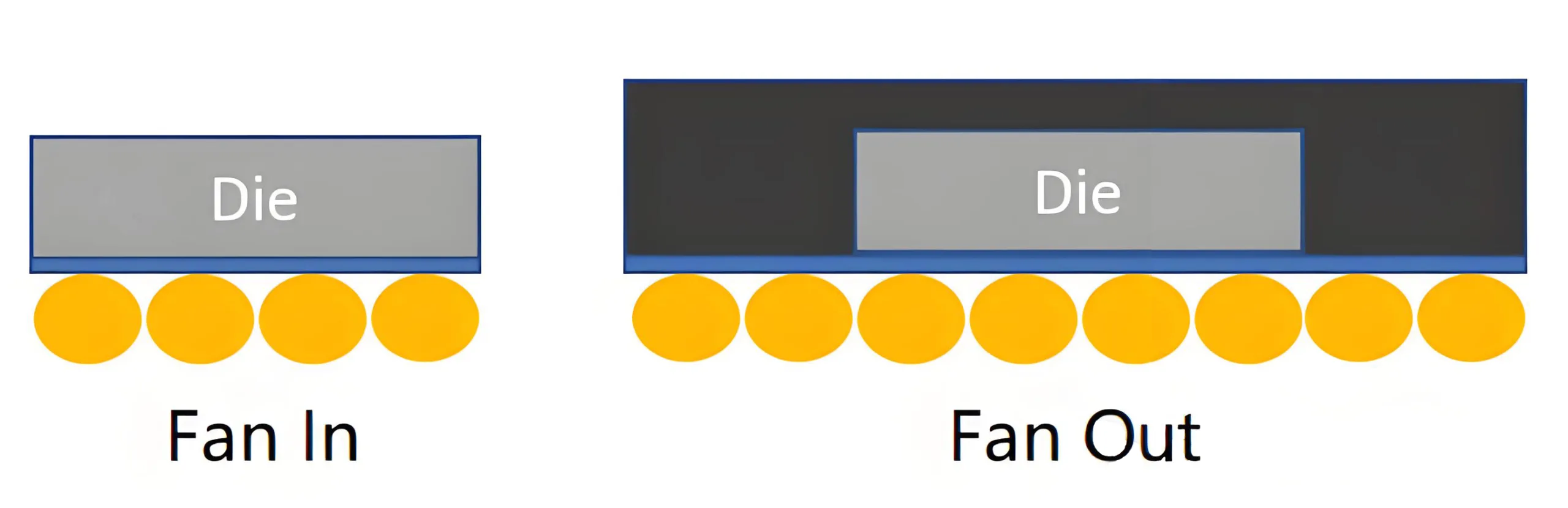
-
Fan-in wlcsp:
-
Boules dans la zone de la matrice
-
Taille du paquet = taille de matrice
-
À faible coût pour les capteurs / PMIC
-
-
Fan-out wlcsp (par ex., Informations TSMC, Samsung FO-PLP):
-
Les balles s'étendent au-delà de la mort
-
Taille de l'emballage > taille
-
Densité d'E / S plus élevée, intégration multi-chip
-
Pour les modules SOC / RF premium
-
ID visuel: Silicium non encapsulé (contre. DFN moulé en résine).
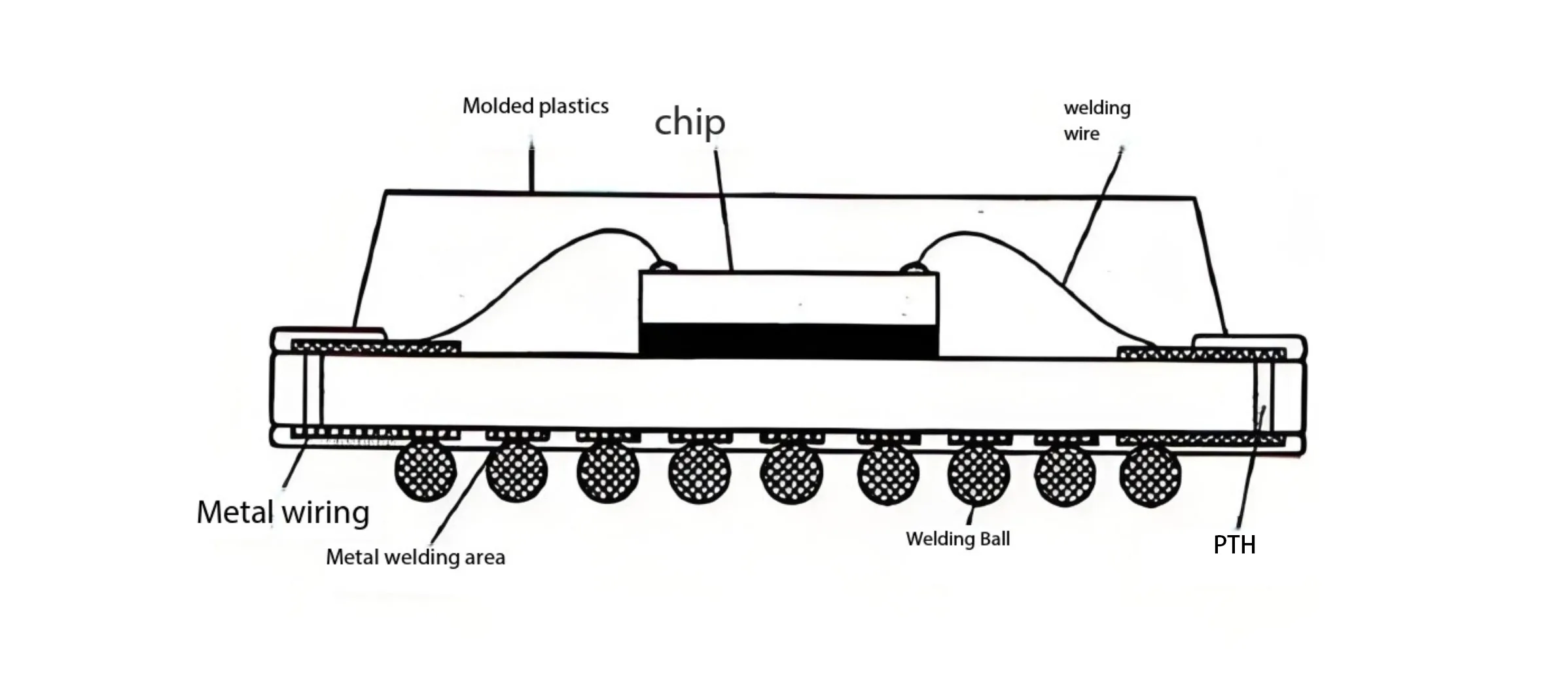
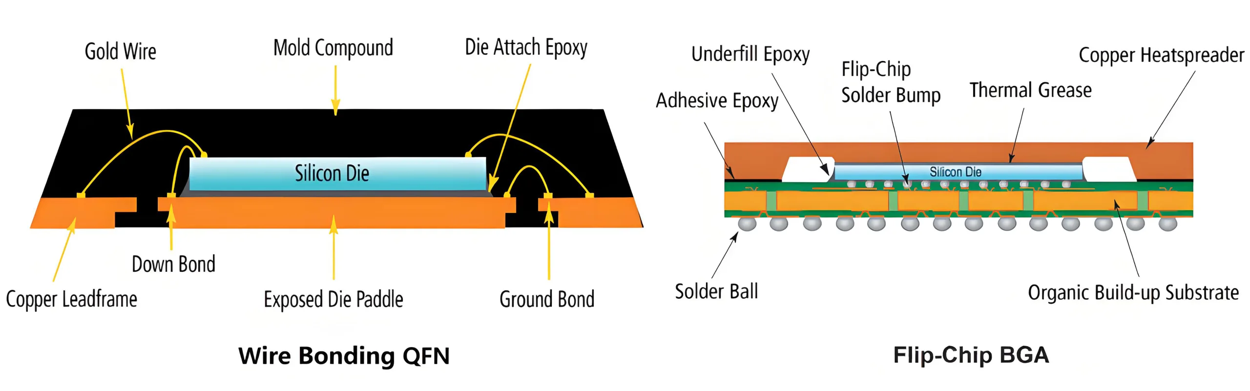
Morphologie des emballages & Techniques de liaison
Formulaire de package externe (QFP / BGA / WLCSP) et la liaison interne sont intrinsèquement liées:
-
Collage de câbles:
-
Mature, faible coût
-
Dominate QFP / QFN / BGAS de milieu de gamme
-
Avoir / avec des fils; E / S modérée
-
-
Plip:
-
Dies attache face face cachée via des microbumps
-
Interconnextes les plus courtes, inductance la plus basse
-
Essential pour FCBGA / WLCSP / CSP haute performance
-
Conclusion & Futures frontières
De QFP à LGA / BGA et enfin CSP / WLCSP, L'évolution des emballages de puces est un Chronique de la compression spatiale, gains de performance, et optimisation des coûts. Chaque saut de miniaturisation remodèle la conception de PCB - conduisant des traces plus fines, multicouche IDH, et matériaux avancés.
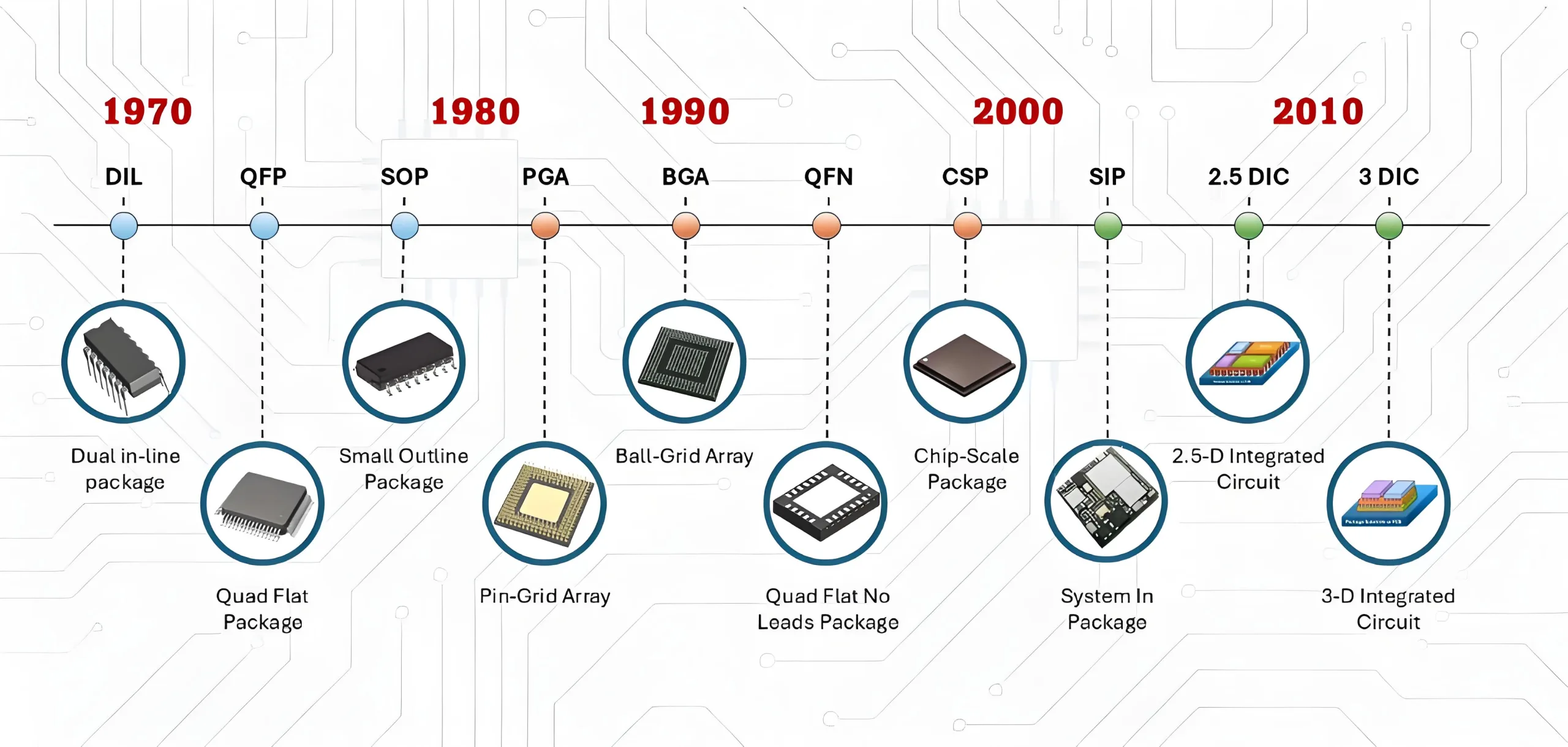
Frontière suivante: Technologies comme TSV (À travers le silicon via), Siroter (Système en pack), et 2.5D / 3D IC permettent désormais une intégration hétérogène 3D, Pousser la conception des PCB dans de nouvelles dimensions - pour être exploré dans notre prochain article.
Lorsqu'un milliard de transistors s'inscrivent dans un ensemble de grains de sable, Battles d'ingénierie électronique à l'échelle moléculaire.

Merci d'avoir partagé l'information avec nous.
whoah ce blog est magnifique j'aime beaucoup lire tes articles. Continuez vos bonnes peintures! Vous reconnaissez, beaucoup de gens recherchent cette information, vous pouvez grandement les aider.