
Dans des modules de puissance compacts, unités de contrôle de véhicules à énergie nouvelle, ou équipements industriels de forte puissance, PCB les designers sont souvent confrontés à un défi de taille: comment gérer en toute sécurité la haute tension dans un espace de carte limité? Une erreur de conception d'espacement apparemment mineure peut entraîner une décharge d'arc, rupture d'isolation, voire des incidents de sécurité. Cet article fournit une analyse approfondie de deux concepts fondamentaux du routage haute tension — la distance de dégagement et la ligne de fuite — et établit une base de sécurité solide pour votre PCB et PCB conception basée sur des normes faisant autorité.
Clarification des concepts: La différence fondamentale entre le jeu et la ligne de fuite
D'abord, il faut définir clairement ces deux concepts de sécurité souvent confondus. Selon IPC-2221B (Norme générique sur Conception de cartes imprimées) et IEC 60664-1 (Coordination de l'isolation des équipements dans les systèmes basse tension):
-
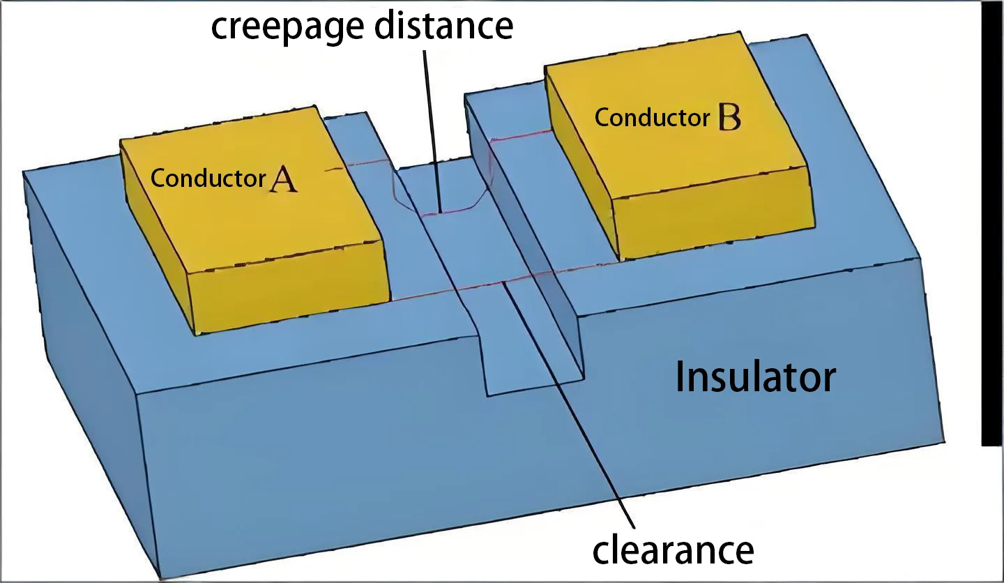
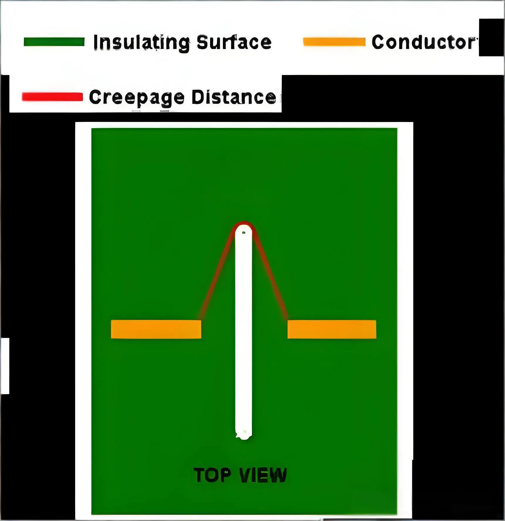
Autorisation: La distance en ligne droite la plus courte dans l'air entre deux pièces conductrices, ou entre une pièce conductrice et le boîtier de l'équipement. Il empêche principalement la dégradation du diélectrique de l'air par la haute tension., provoquant un arc instantané. Considérez-le comme le “distance en ligne droite pour traverser un canyon.”
-
Distance d'isolement: La longueur de trajet la plus courte le long de la surface d'un matériau isolant entre deux parties conductrices. Il prévient principalement les contaminants (comme la poussière, humidité, résidu de flux) de former un chemin conducteur sur la surface isolante, conduisant à une fuite lente ou à un échec de suivi. Cela s'apparente au “le chemin le plus court pour qu'une fourmi rampe le long de la paroi du canyon.”
La principale distinction réside dans le support: on compte sur l'air, l'autre concerne l'état de la surface isolante. Dans des environnements avec des degrés de pollution plus élevés, les exigences de distance dans l'air sont souvent plus strictes que les distances dans l'air.
Pierre angulaire du design: Normes faisant autorité et spécifications de conception de PCB basées sur les données
La conception sans normes est aveugle. Pour la haute tension Conception de circuits imprimés, les ingénieurs doivent suivre les normes de sécurité correspondantes (par ex., UL, IEC, FR) basé sur le domaine d'application du produit (comme l'électronique grand public, contrôle industriel, dispositifs médicaux, électronique automobile). Parmi ceux-ci, IEC 60664-1 est une norme internationale fondamentale qui fournit une méthode de conception de table de recherche basée sur la tension de fonctionnement, degré de pollution, groupe de matériaux, et catégorie de surtension.
Prendre une alimentation à découpage AC-DC typique (entrée 100-240VAC, avec circuit PFC) isolation de sécurité entre les côtés primaire et secondaire à titre d'exemple, ses exigences en matière d'isolation comprennent généralement:
-
Isolation de base: Protection fondamentale contre les chocs électriques.
-
Isolation renforcée: Equivalent à une double isolation de base, offrant une plus grande fiabilité.
Selon IEC 62368-1 (Norme de sécurité pour l'audio/vidéo, Équipement des technologies de l’information et de la communication) et exigences communes en matière de certification, sous Degré de pollution 2 (environnement industriel général), pour une tension de travail de 240ACC (tension de crête correspondante ~ 340 V), les exigences minimales en matière de ligne de fuite et de dégagement sont généralement les suivantes:
| Type d'isolation | Autorisation (Min.) | Distance d'isolement (Min., Groupe de matériaux IIIa) |
|---|---|---|
| Isolation de base | 2.0 mm | 3.2 mm |
| Isolation renforcée | 4.0 mm | 6.4 mm |
(Note: Les valeurs ci-dessus sont typiques. La conception réelle doit suivre le processus complet de table de recherche de la norme choisie, en tenant compte de facteurs tels que l'altitude et les surtensions transitoires.)
Solutions pour un parc immobilier limité en PCB: Cinq stratégies d'ingénierie
Lorsque l’espace sur le tableau est restreint et que les exigences de distance en ligne droite ne peuvent pas être respectées, expérimenté Conception de PCBA les ingénieurs emploient les stratégies suivantes pour augmenter efficacement la longueur de la ligne de fuite:
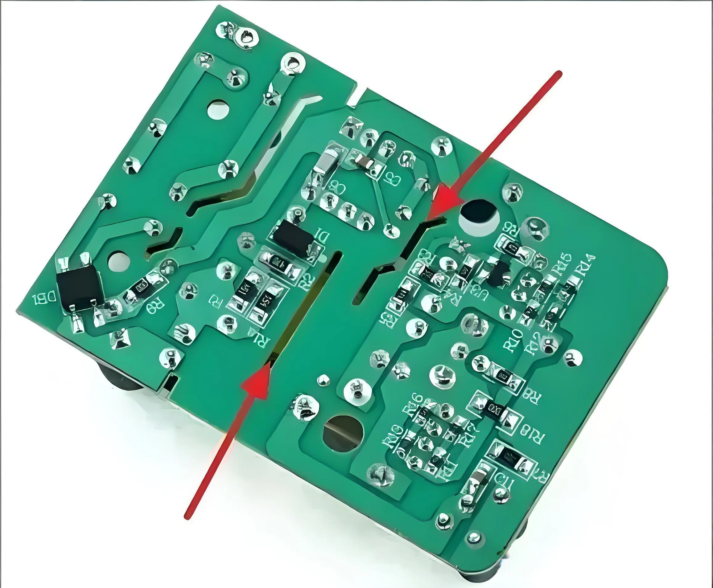
1. Rainurage pour augmenter la distance
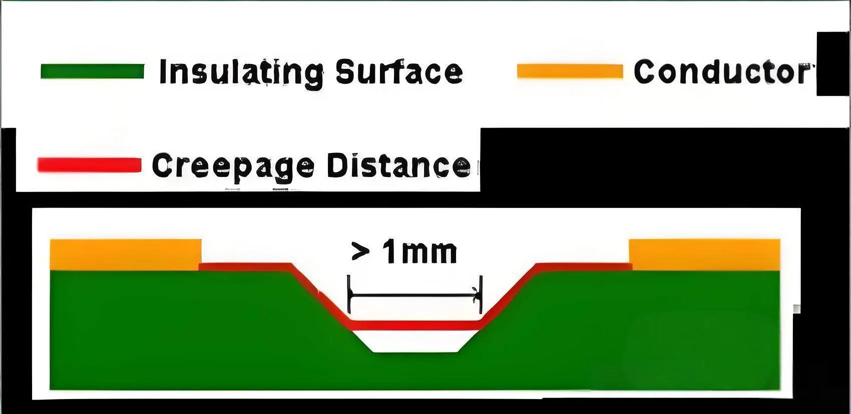
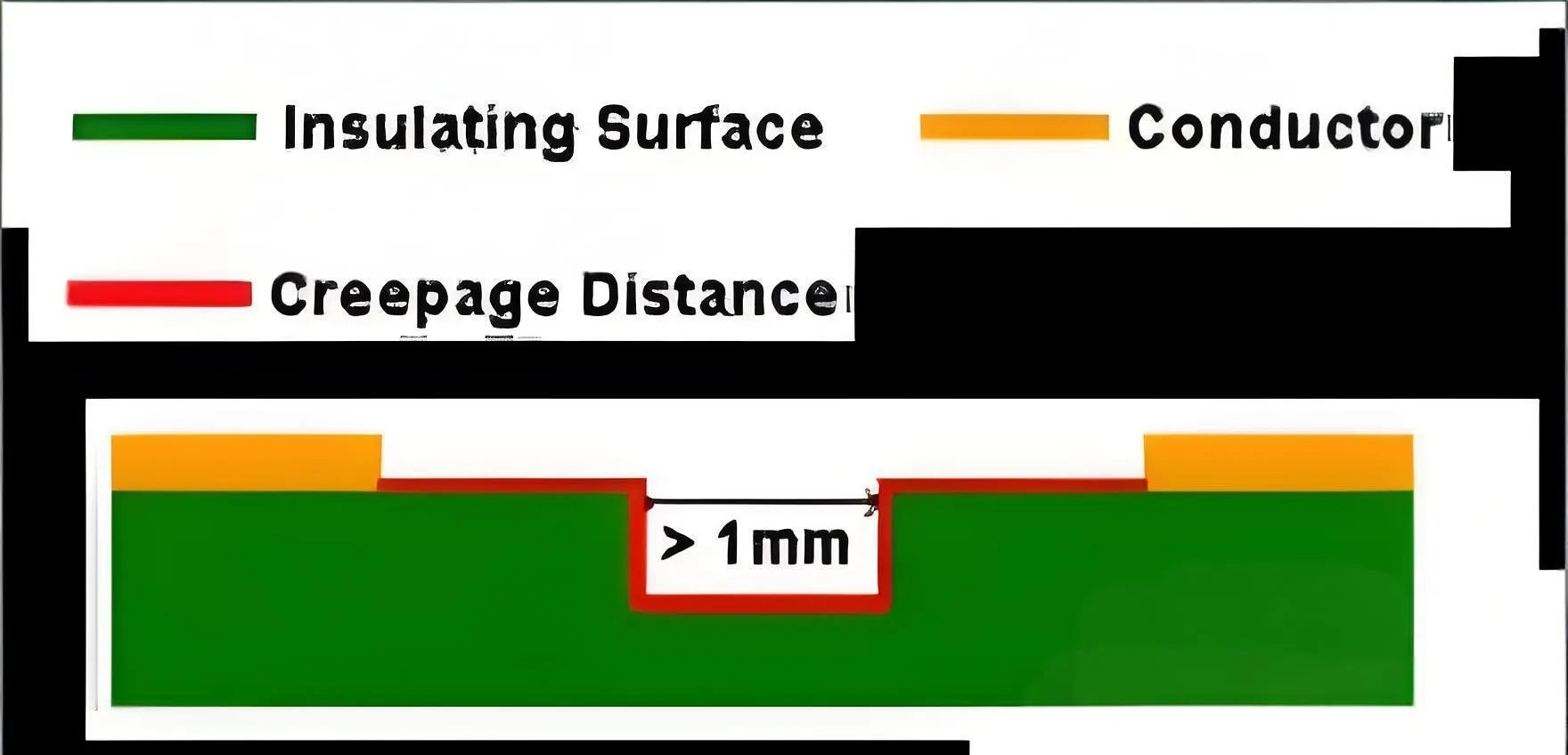
C'est la méthode d'ingénierie la plus classique et la plus efficace. Fraisez ou percez une fente d'isolation dans la zone de coulée de cuivre entre deux conducteurs haute tension..
-
Rainure en V / Rainure en U: Convient pour une compensation de distance modérée. La fente ne pénètre pas dans le PCB; la profondeur est généralement 1/3 à 2/3 de l'épaisseur du panneau. Cela force effectivement la ligne de fuite à dévier le long de la paroi de la fente., augmentation significative de la distance à la surface.
-
Longue fente traversante: Le plus efficace. Une fente d'isolation complètement pénétrante (souvent largeur ≥1.0mm) est créé directement entre les conducteurs. La ligne de fuite doit parcourir toute la longueur de la fente, augmentant la distance de plus de deux fois la largeur de la fente. Il s'agit d'une technique courante dans les circuits imprimés d'alimentation à découpage pour isoler les côtés primaire et secondaire..
2. Mise à niveau du matériel PCB
-
Sélectionnez Haute Performance Substrat PCB: L'indice de suivi comparatif (CTI) de la norme FR-4 varie généralement de 175 à 250 V. Choisir des matériaux à CTI élevé (par ex., matériaux d'isolation de sécurité dédiés avec CTI ≥600V) permet des exigences de distance dans l'air plus courtes selon les normes CEI. Par exemple, Groupe de matériaux I (CTI ≥600V) peut nécessiter près de la moitié de la ligne de fuite du groupe IIIa (100V ≤ CTI <175V).
-
Utiliser des substrats en céramique: Pour les conceptions à très haute densité de puissance, tels que les modules pilotes IGBT dans les PCB automobiles, utiliser directement l'alumine (Al₂O₃) ou nitrure d'aluminium (AIN) substrats en céramique. Les céramiques ont non seulement un CTI extrêmement élevé, mais également une excellente conductivité thermique, éliminant fondamentalement les risques de suivi de surface.
3. Amélioration du revêtement de surface des PCB
Appliquer un revêtement conforme ou une peinture anti-trace spécialisée sur les zones à haute tension du PCB. Cela peut améliorer la résistance de l'isolation de surface et résister dans une certaine mesure à l'humidité et à la contamination.. Cependant, notez que la plupart des normes de sécurité (par ex., UL) ne permettent pas de compter uniquement sur les revêtements pour réduire la ligne de fuite. Il s'agit plutôt d'une méthode de renforcement auxiliaire, et la qualité du revêtement et la fiabilité à long terme doivent être validées.
4. Pensée de conception tridimensionnelle
Pensez au-delà de la disposition du plan 2D; utiliser la troisième dimension.
-
Utiliser des murs/barrières isolants: Souder des cloisons en plastique isolantes sur le PCB.
-
Utiliser des cavaliers ou des isolateurs montés verticalement: Réalisez des connexions haute tension via des fils volants (autorisation satisfaisante), évitant complètement les problèmes de fuite en surface.
5. Points clés du processus de transformation
Dans la conception d'une alimentation à découpage isolée, l'isolation interne du transformateur est critique. Fil à triple isolation ou parois de bobine suffisantes (flotte) doit être utilisé entre les enroulements primaire et secondaire. La distance d'isolement est égale à la somme des largeurs des murs des deux côtés plus l'entrefer sur la longueur de l'enroulement. Les broches doivent être gainées avec un tube isolant, et le tube doit traverser la paroi de la canette pour éviter “raccourci” panne au niveau des broches.
Vérification de la conception et tendances futures
Une fois la conception terminée, vérification stricte à l'aide DFM (Conception de la fabrication) et DFA (Conception pour l'assemblage) les règles sont essentielles, spécialement pour les sections haute tension. Professionnel Fabricants de PCB et les fournisseurs de PCBA doivent posséder les capacités correspondantes d'examen des normes de sécurité.
En avant, à mesure que les tensions des appareils augmentent et que les tailles diminuent, la prolifération des semi-conducteurs à large bande interdite comme SiC (Carbure de silicium) et GaN (Nitrure de Gallium) pose des défis plus stricts en matière de tension de tenue des PCB et de conception thermique. L'utilisation d'un logiciel de simulation pour l'analyse préalable de la distribution du champ électrique deviendra le processus standard pour la conception de circuits imprimés de puissance haut de gamme..
Conclusion
La conception de sécurité pour le routage haute tension est le reflet concentré du professionnalisme et du sens des responsabilités d'un ingénieur PCB.. Dégagement et ligne de fuite – ces deux éléments invisibles “lignes rouges de sécurité” — garantir la fiabilité à long terme du produit et, plus important encore, la sécurité des utilisateurs finaux’ vies et biens. Dans la recherche actuelle de densité de puissance et d’efficacité, la maîtrise de ces principes de sécurité et l'application flexible de solutions d'ingénierie constituent un obstacle technique crucial que tout praticien engagé dans la conception de PCB haute tension et la fabrication de PCBA de haute qualité doit surmonter.. Face à de tels défis de conception, professionnel du conseil Fournisseurs de PCB ou des prestataires de services PCBA avec une riche expérience en matière de normes de sécurité, comme l'UGPCB, car la collaboration en matière de conception dès les premières étapes est sans aucun doute la meilleure voie pour atténuer les risques et optimiser les coûts.
