
Introduction: Le rôle essentiel du contrôle environnemental dans les PCB/PCBA
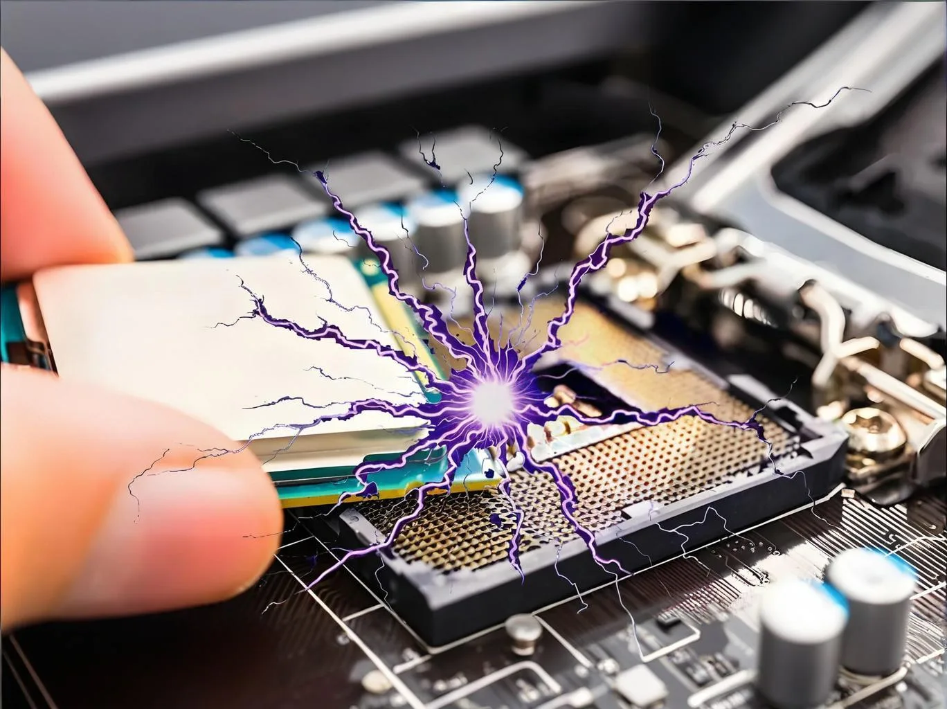
Un léger crépitement de décharge électrostatique peut détruire instantanément un microprocesseur précieux.. Tu as oublié BGA composants, exposé à l'air humide, peut s'oxyder silencieusement, conduisant à des défauts de soudure. Ces menaces cachées représentent des défis importants en matière de gestion environnementale qui ne peuvent être ignorés dans Fabrication de PCB.
Dans le domaine des PCB et PCB fabrication, Décharge électrostatique (ESDE) et appareil sensible à l'humidité (MSD) la gestion sont des facteurs critiques ayant un impact sur la fiabilité du produit et le rendement au premier passage. Alors que les appareils électroniques tendent vers la miniaturisation et une densité plus élevée, les risques potentiels posés par les ESD et les composants sensibles à l'humidité deviennent encore plus prononcés.
Les données statistiques indiquent que plus 60% des incendies électriques et des incidents de choc électrique dans les systèmes basse tension sont causés par des défauts de mise à la terre, en particulier les défauts d'arc. En outre, environ 30% des accidents de choc électrique sont liés à l’absence de DDR (Appareils à courant résiduel) ou sélection incorrecte du RCD. La gestion efficace des ESD et des TMS est fondamentale pour atténuer ces risques dans PCB production.
Protection ESD: Des principes fondamentaux à l’application pratique
Décharge électrostatique (ESDE) est un sujet vital dans le cadre de la compatibilité électromagnétique (CEM), en particulier pour l'électronique moderne où les événements ESD peuvent provoquer un dysfonctionnement de l'équipement, perte de données, ou des dommages matériels permanents. La mise en œuvre de mesures de contrôle ESD robustes est essentielle pour tout fabricant de PCB sérieux.
Mécanismes ESD et modèles de dommages
L'ESD affecte les équipements électroniques principalement à travers trois mécanismes: effets de conduction directe via les E/S ou les ports d'alimentation; effets de couplage de champ par couplage radiatif en champ proche; et les effets des impulsions électromagnétiques dus à des transitoires rapides, interférence électromagnétique à large bande.
Dans l'environnement de fabrication de PCB, L'ESD se produit principalement dans trois modes de décharge:
-
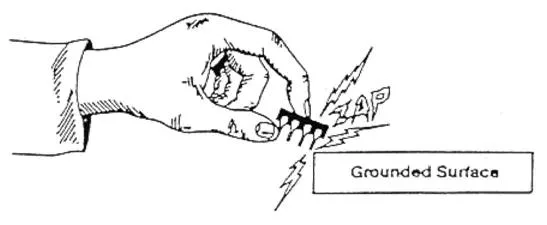
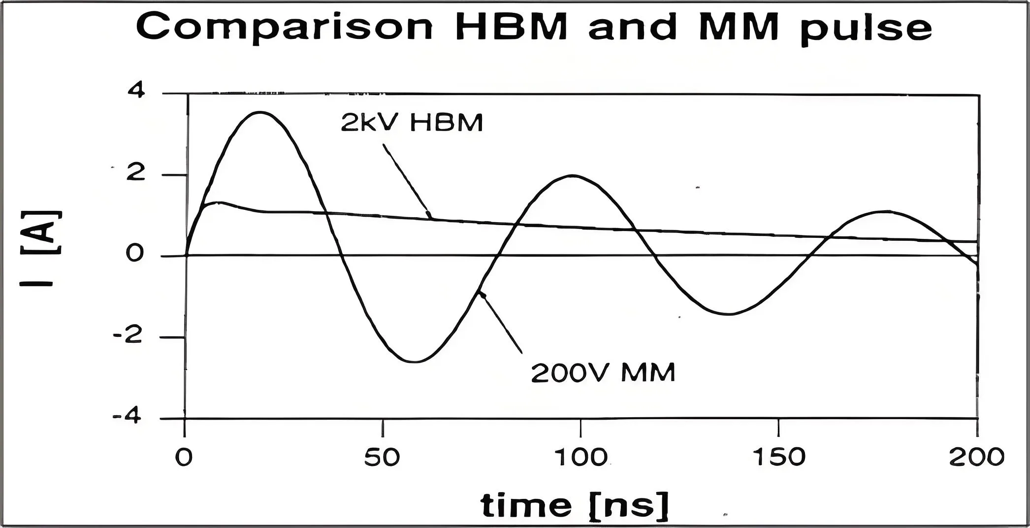
Modèle de corps humain (HBM): Une personne accumule une charge statique par mouvement ou friction. En touchant un circuit intégré (CI), la charge électrostatique stockée se décharge à travers les broches du circuit intégré jusqu'à la terre. Cette décharge peut générer une surtension de plusieurs ampères en quelques centaines de nanosecondes.
-
Modèle de machine (MM): Les machines elles-mêmes accumulent une charge statique. Lorsque la machine entre en contact avec un IC, la décharge électrostatique se produit à travers les broches du circuit intégré. Comme les machines sont généralement en métal, la résistance de décharge équivalente est très faible, ce qui entraîne un processus de décharge encore plus rapide : plusieurs ampères en quelques nanosecondes jusqu'à des dizaines de nanosecondes.
-
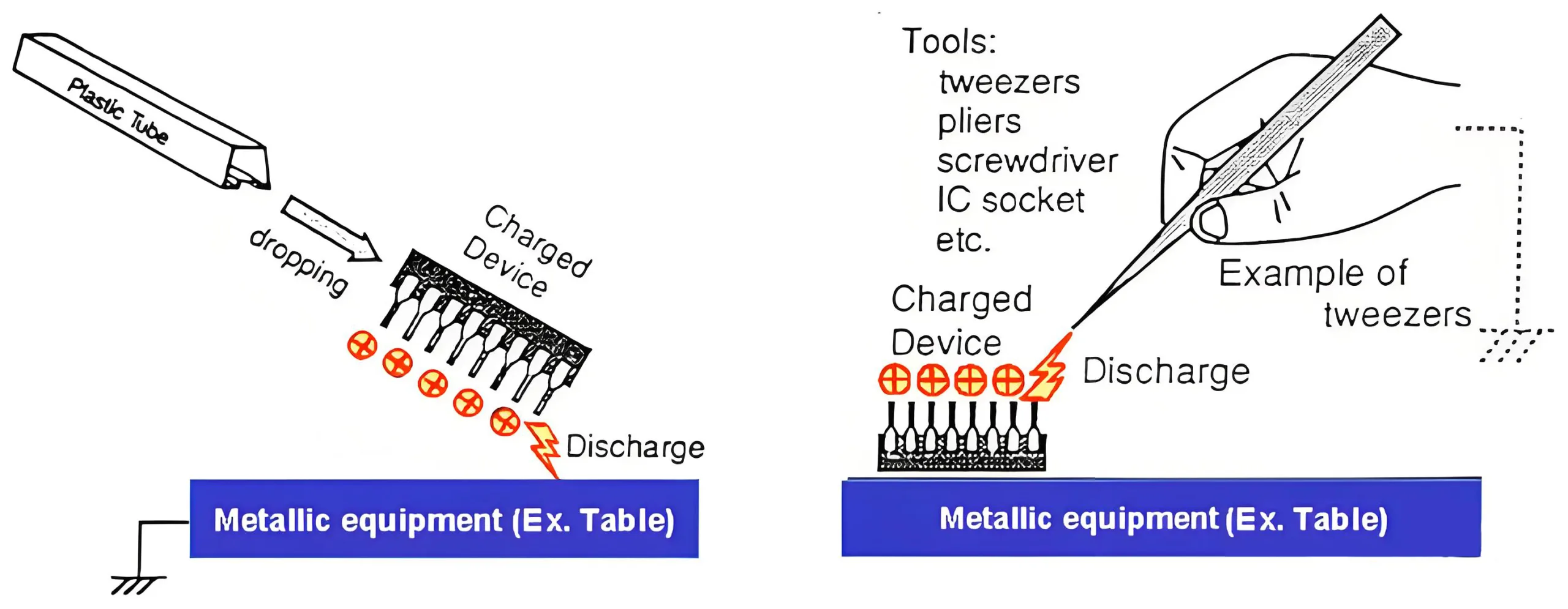
Modèle d'appareil chargé (MDP): Un circuit intégré accumule une charge statique interne via la friction ou d'autres moyens sans dommage immédiat. Ensuite, lorsqu'une broche du circuit intégré chargé entre en contact avec une surface mise à la terre, la charge statique interne s'écoule rapidement à travers la broche, provoquant un événement de décharge.
Matériaux de protection ESD et normes de mise à la terre
Une protection ESD efficace repose sur des matériaux appropriés et des méthodologies scientifiques fondées. Les métaux sont conducteurs et peuvent endommager les composants en raison de courants de fuite élevés.. Les isolants sont sujets à la charge triboélectrique. Donc, ni les métaux purs ni les isolants ne sont des matériaux de protection ESD idéaux. Plutôt, les matériaux utilisés comprennent des conducteurs électrostatiques (résistivité superficielle < 1×10⁵ Ω·cm) et matériaux dissipateurs électrostatiques (résistivité superficielle comprise entre 1×10⁵ Ω·cm et 1×10⁸ Ω·cm).
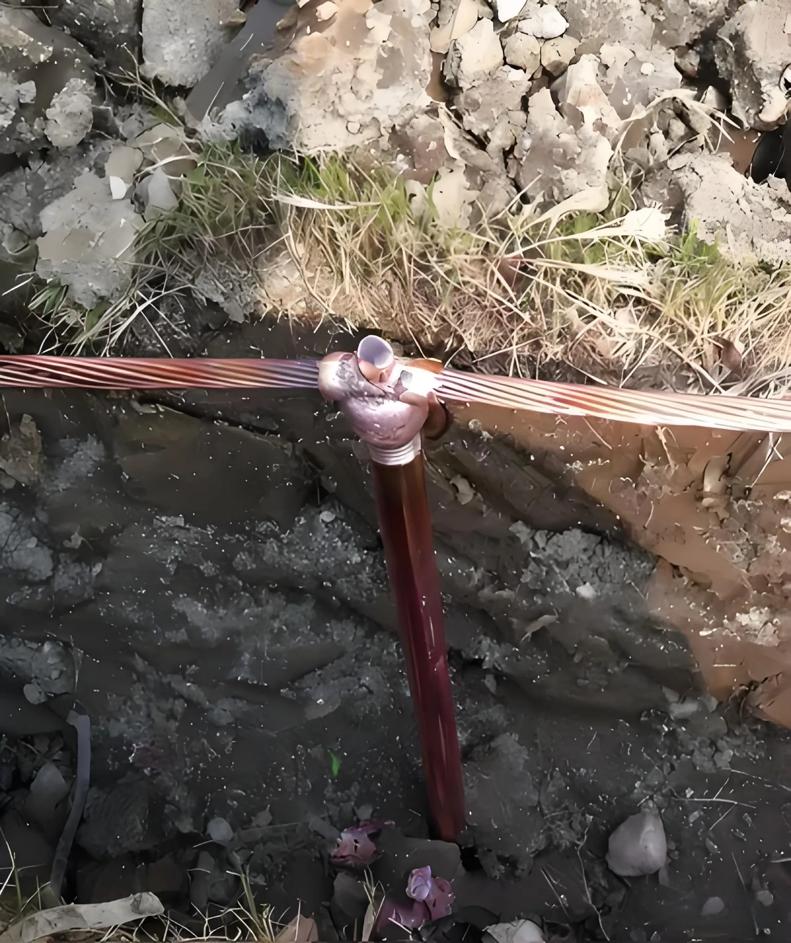
La mise à la terre est la pierre angulaire de la protection ESD. Selon les normes communes, la résistance d'une électrode de terre ESD doit généralement être inférieure à 4 Ω (avec quelques normes, comme certaines normes américaines, exigeant <1Oh). Un système de mise à la terre robuste utilise souvent une approche multipoint: au moins trois points au sol espacés 3-5 mètres l'un de l'autre, utilisant des tiges d'acier recouvertes de cuivre enfoncées verticalement sur 2 mètres dans des fosses de plus de 0,5 m de profondeur. Ces points sont reliés entre eux par un conducteur toronné de 70 mm², et un fil de cuivre isolé de 16 mm² est connecté de cette grille à l'intérieur de l'installation comme bus de terre principal..
Les exigences en matière de mise à la terre des surfaces de travail et des zones sont encore plus strictes: Les fils de terre ESD doivent utiliser un fil de cuivre isolé multibrins de 6 mm², et la résistance entre tout point de test ESD et le bus de terre ESD principal doit être maintenue entre 5 et 15 Ω..
Normes et méthodes de test ESD
La Commission Electrotechnique Internationale (IEC) norme CEI 61000-4-2 régit l’immunité des équipements électroniques aux ESD. Le 2025 Cette édition introduit des exigences d'immunité plus strictes et des méthodes/paramètres de test mis à jour pour répondre aux besoins des appareils électroniques les plus récents..
Les tests ESD sont principalement effectués selon deux modes: Décharge de contact et décharge d'air. La décharge par contact simule le contact direct entre un utilisateur/objet et l'équipement, avec une tension d'essai typique de 8kV. La décharge d'air simule une étincelle sans contact provenant d'un utilisateur/objet chargé s'approchant de l'équipement, avec une tension d'essai typique de 15kV.
(H3) Niveaux de test ESD selon CEI 61000-4-2 Standard
| Niveau de test | Contacter la décharge (kv) | Décharge d'air (kv) |
|---|---|---|
| 1 | 2 | 2 |
| 2 | 4 | 4 |
| 3 | 6 | 8 |
| 4 | 8 | 15 |
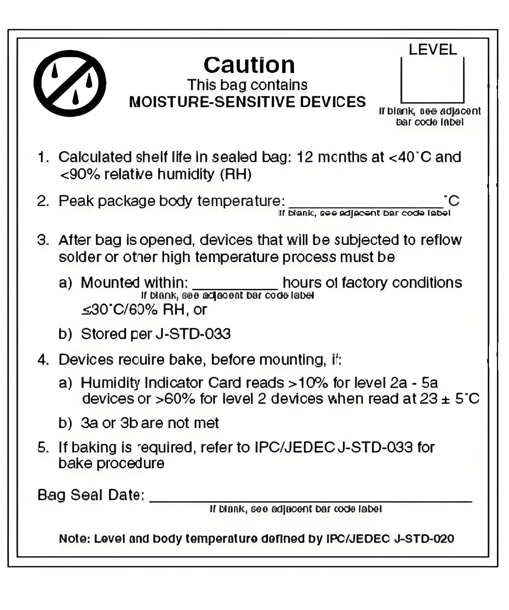
Appareil sensible à l'humidité (MSD) Gestion: Contrôle complet, de l'identification à la cuisson
La gestion des TMS est un autre élément de contrôle critique dans CMS environnements. Un mauvais contrôle de l'humidité peut entraîner “effet pop-corn” pendant le brasage par refusion, où l'humidité interne se vaporise rapidement, provoquant un délaminage et des fissures dans le composant.
Identification et classification des TMS
Les appareils sensibles à l'humidité sont des composants susceptibles d'être endommagés par l'humidité., comprenant principalement des PCB et des circuits intégrés (par ex., BGA, CFP). Ils sont classés en huit niveaux (1, 2, 2un, 3, 4, 5, 5un, 6), chacun avec des exigences spécifiques en matière de durée de vie au sol.
La durée de vie au sol fait référence à la durée autorisée pendant laquelle un MSD peut être exposé aux conditions du sol de l'usine après l'ouverture de son sac scellé.. Cela va de 1 année (Niveau 2) à exiger une cuisson immédiatement avant utilisation (Niveau 6). Une identification et une classification correctes sont des conditions préalables à une gestion efficace.
Spécifications de stockage et de manipulation des MSD
Les environnements de stockage pour les MSD nécessitent un contrôle strict. La température de l'entrepôt doit être ≤30°C, avec une humidité contrôlée entre ≤85%RH et ≤70%RH selon le niveau de MSD.
Les exigences d’emballage varient selon le niveau: Les niveaux 1-2a n'ont pas d'exigences particulières; Les niveaux 3 à 5a nécessitent des sacs barrière contre l'humidité., déshydratant, et étiquettes d'avertissement; Niveau 6 nécessite une étiquette d'avertissement mais pas de sac barrière contre l'humidité.
Une fois ouvert, Les MSD doivent être utilisés strictement pendant leur durée de vie au sol spécifiée.. Le personnel de production doit déterminer la quantité à ouvrir en fonction du calendrier de production. Dès l'ouverture, un “Carte de contrôle des composants MSD” doit être attaché. Tous les composants non utilisés immédiatement doivent être stockés temporairement dans une armoire sèche. (25±5°C, ≤30% HR).
Procédures de cuisson MSD
La cuisson est requise lorsque les MSD dépassent leur temps d'exposition autorisé ou lorsque la carte indicatrice d'humidité (HIC) indique des niveaux d'humidité dépassant la norme (par ex., >30%Rh). La cuisson est nécessaire dans ces conditions:
-
L’emballage sous vide entrant est endommagé ou fuit.
-
HIC affiche une humidité supérieure à 30 % HR.
-
Les composants dépassent leur durée de stockage scellée spécifiée par le fabricant.
-
Les composants ouverts dépassent leur durée de vie au sol spécifiée.
-
Les exigences spécifiques du client imposent la cuisson.
Les paramètres de cuisson sont déterminés par les propriétés des composants:
-
TMS avec emballage résistant aux hautes températures: 115-125° C.
-
TMS dont l'emballage ne supporte pas les températures élevées: 35-45° C.
Les exigences en matière de cuisson des PCB sont spécifiques: PCB avec finition OSP stockés pendant plus de 6 mois, et ENIG (Immersion Or) finir les PCB stockés pendant plus de 9 mois, nécessiter une cuisson. Les PCB OSP sont généralement cuits à 70-80°C pendant 3-6 heures, tandis que les PCB ENIG sont cuits à 115-125°C pendant 3-6 heures.
Mesures de protection ESD dans la conception de circuits imprimés
Supérieur Conception de circuits imprimés constitue la base de la protection ESD. Une disposition et un routage rationnels peuvent améliorer considérablement l’immunité ESD d’un produit.
Stratégie d'empilement et directives de routage
Pour un empilement de PCB à 4 couches, la configuration recommandée est Signal-GND-Power-Signal, s'assurer que les traces de signaux critiques font référence à un plan de masse solide. Pendant le routage, les traces de signaux sensibles doivent être conservées à ≥ 5 mm du bord de la carte. L'inadéquation de longueur pour les paires différentielles doit être contrôlée dans un délai ≤ 5 mm. Les signaux critiques doivent éviter de traverser des plans divisés.
Pour les PCB RF, nécessitent une mise à la terre sur une grande surface. Dans les circuits microrubans, la couche inférieure doit être lisse, plan de sol continu. Les surfaces de contact avec la terre doivent être plaquées d'or ou d'argent pour garantir une bonne conductivité et une faible impédance..
Conception et mise en œuvre du blindage
Les circuits sensibles et les radiateurs puissants nécessitent un blindage. Zones de circuits telles que les frontaux des récepteurs, Unités RF/IF, oscillateurs, amplificateurs de puissance, alimentations d'antenne, et les processeurs de signaux numériques nécessitent souvent un blindage approprié.
Les matériaux de blindage courants sont hautement conducteurs, tels que des plaques/feuilles de cuivre, plaques/feuille d'aluminium, tôles d'acier, placages métalliques, et revêtements conducteurs. Sur le PCB lui-même, un “Via une clôture” peut être mis en œuvre: placez des rangées de vias mis à la terre le long de la zone où un blindage peut entrer en contact avec le PCB. Nécessite au moins deux rangées de vias décalées, avec un espacement entre les vias d'une même rangée inférieur à λ/20.
Exigences de mise à la terre et de sécurité du système
La mise à la terre du système est la base pour garantir la sécurité dans tout l'environnement de fabrication électronique.. Les normes nationales pertinentes sont en cours de révision pour étendre leur champ d'application des systèmes CA basse tension aux systèmes hybrides CC et CA/CC., ajout d'exigences de mise à la terre et de sécurité pour les systèmes CC basse tension.
Conception et mise en œuvre du système de mise à la terre
La conception du système de mise à la terre doit équilibrer sécurité et fiabilité. La résistance de terre du système doit être inférieure à 4 Ω selon les normes communes. Les électrodes de mise à la terre doivent être placées au moins 10 mètres des fondations du bâtiment et des supports d'équipement pour éviter l'influence de “tension de pas” lors des coups de foudre.
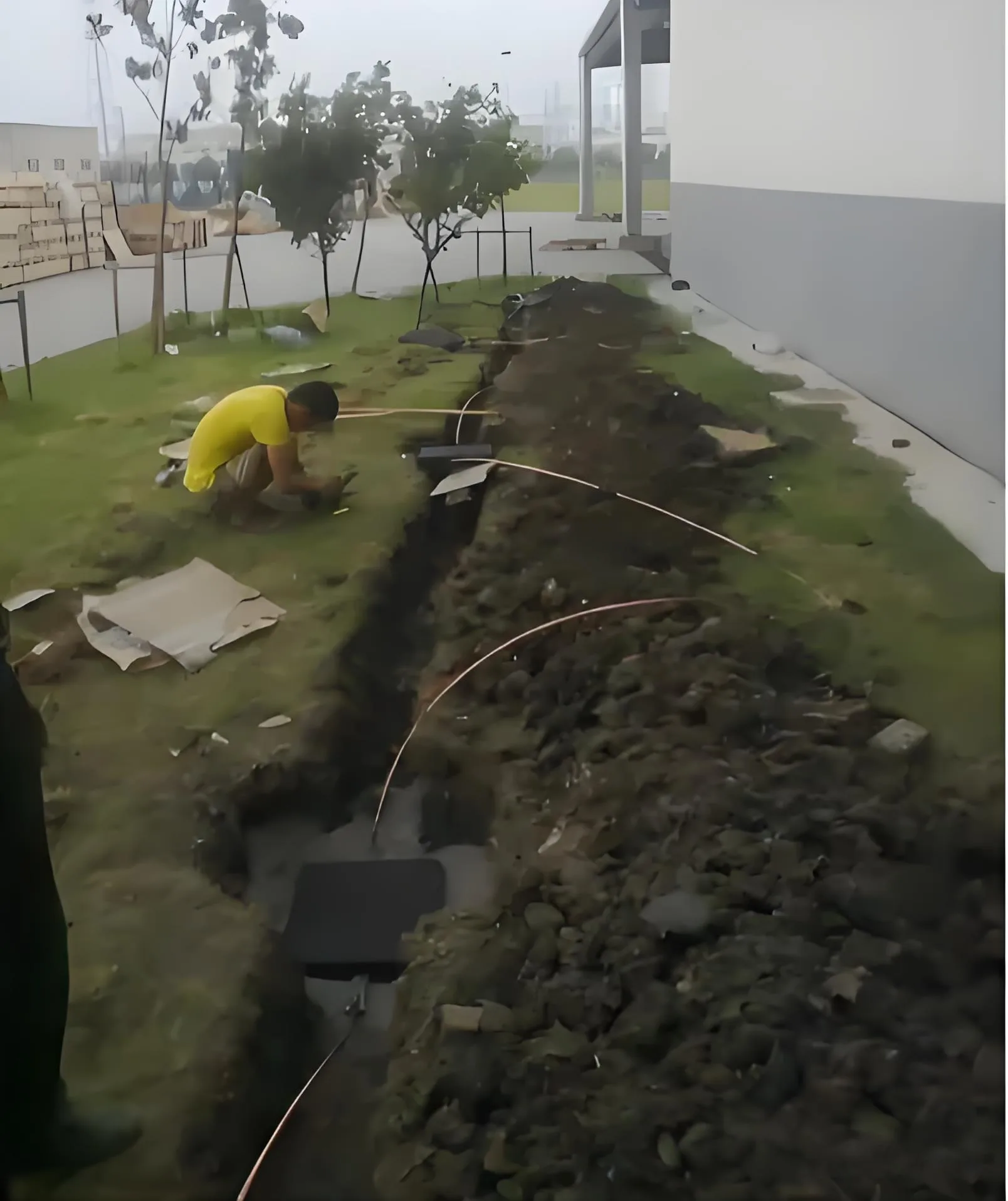
L'installation doit suivre des procédures strictes: Électrodes de terre ESD (par ex., 3tiges cuivrées m×φ20mm) sont enfoncés verticalement jusqu'à une profondeur d'au moins 3 m sous le niveau de la surface. Au moins trois électrodes sont disposées en ligne avec 3-5 espacement en mètres, entouré de matériaux d'amélioration du sol.
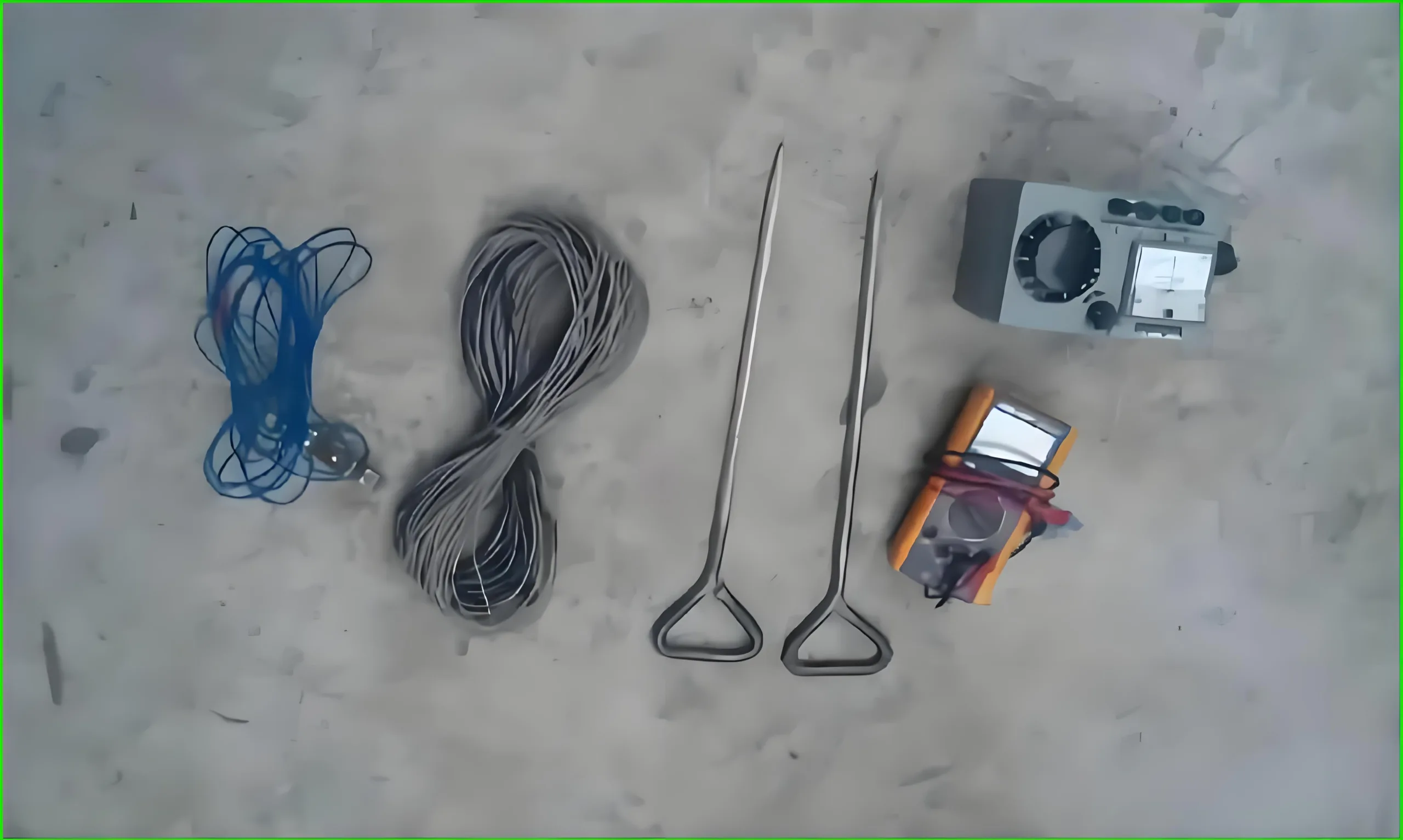
Test et vérification de la résistance au sol
L'efficacité du système de mise à la terre doit être vérifiée par des tests périodiques. Utilisation d'un testeur de résistance de terre, les sondes de test sont insérées dans le sol au moins 10 mètres l'un de l'autre, et la valeur de résistance est mesurée.
Les tests doivent être effectués au moins une fois par an pour garantir la fiabilité du système. Tous les résultats des tests doivent être enregistrés et analysés pour détecter les tendances afin d'identifier les problèmes potentiels de manière proactive..
Pratiques intégrées de gestion des ESD et des TMS
Exigences de contrôle environnemental
La gestion ESD et MSD exigent des contrôles environnementaux stricts. La température dans une zone protégée ESD (EPA) doit être maintenu à 23 ± 3°C, avec une humidité relative comprise entre 45 et 70 % HR. Utilisation d'appareils sensibles aux ESD (SSD) dans des environnements inférieurs à 30 % HR est interdit.
Les zones de production doivent être maintenues propres. Objets personnels comme de la nourriture, boisson, sacs, lainages, journaux, et les gants en caoutchouc sont interdits sur les surfaces de travail de l'EPA.
Formation du personnel et procédures opérationnelles
Tout le personnel manipulant des TMS doit porter des gants et des dragonnes ESD., mettre en œuvre des mesures complètes de protection contre les décharges électrostatiques. Les opérateurs nécessitent une formation en matière de sécurité ESD et doivent passer les contrôles pertinents avant d'être autorisés à produire..
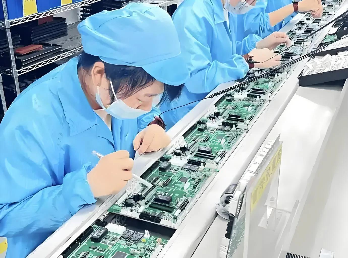
Les opérateurs doivent porter un bracelet ESD fonctionnel, vérifié quotidiennement. Pour les TMS, les opérateurs doivent suivre strictement le calendrier de production pour déterminer les quantités à ouvrir, éviter une exposition inutile.
Audit et amélioration continue
La mise en place d’un mécanisme d’audit robuste est essentielle au maintien d’une gestion efficace des ESD et des TMS.. IPQC (Contrôle de qualité en cours) doit auditer les cartes de contrôle MSD sur la ligne de production, vérifier qu'ils sont correctement complétés et correspondent aux opérations réelles, corriger rapidement toute non-conformité.
Mesurer régulièrement la résistance superficielle des sols, surfaces de travail, et des conteneurs pour garantir que tous les contrôles ESD sont fonctionnels. Pour tout problème identifié, mettre en œuvre des actions correctives et suivre leur efficacité.
Conclusion: Construire les bases d'une fabrication fiable de PCB
La protection ESD et la gestion des TMS dans la fabrication de PCB constituent un défi d'ingénierie systématique, nécessitant un contrôle complet sur toute la conception, matériels, processus, environnement, et personnels. À mesure que la technologie électronique évolue, grâce aux progrès des nouvelles énergies, bâtiments intelligents, Micro-réseaux DC, etc. — les exigences en matière de mise à la terre et de sécurité du système continuent d'augmenter.
L'établissement d'un système de gestion scientifique et le strict respect des normes et spécifications pertinentes sont les seuls moyens d'améliorer efficacement la fiabilité des PCB/PCBA., améliorer le rendement au premier passage, réduire les risques liés à la qualité, et conserver un avantage concurrentiel. Pour Fabricants de PCB, la mise en œuvre d'un système de gestion ESD et MSD robuste pour améliorer considérablement la fiabilité des produits n'est pas simplement une nécessité pour répondre aux demandes des clients, mais une voie cruciale pour renforcer la compétitivité de base et établir une base solide pour une croissance commerciale durable..

tu es mon inspiration , Je possède peu de journaux Web et je manque rarement d'une marque à l'autre : (.