
Dans l'industrie de la fabrication d'électronique en évolution rapide, CMS défauts de désactivation (communément appelé l'effet de Manhattan ou les défauts de pierre tombale) restent un goulot d'étranglement critique limitant les améliorations dans les domaines des PCB et PCB rendement de premier passage. Alors que les progrès basés sur l'IA propulsent des mises à niveau complètes de la technologie des PCB, innovations dans les matériaux, processus, et les architectures ouvrent la voie à un nouveau cycle industriel. L'adoption généralisée de composants de puces miniatures, tel que 0402 (01005) forfaits, a conduit à une résurgence du phénomène Manhattan avec des taux d'occurrence plus élevés, émergeant comme un défi incontournable dans la fabrication haut de gamme. Cet article fournit une analyse approfondie des causes de désactivation basée sur les données internationales. Normes IPC et modèles mécaniques, tout en proposant une stratégie de prévention complète englobant la conception, matériels, et optimisation des processus.
Le phénomène Manhattan: Le tueur invisible du soudage CMS
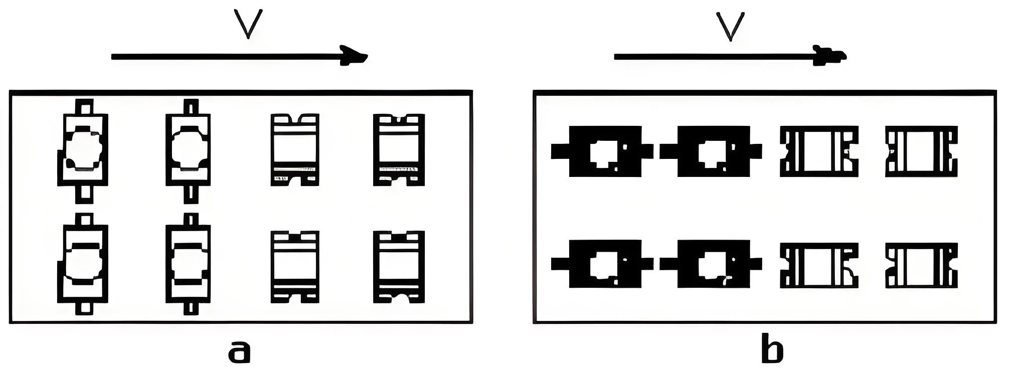
Le phénomène Manhattan est un défaut courant dans le soudage par refusion CMS, où une extrémité d'un composant de puce se soulève du tampon, tournant verticalement selon un angle (généralement 30°–90°), ressemblant à un gratte-ciel ou à une pierre tombale, d'où son nom. Ce défaut compromet non seulement la connectivité électrique mais peut également entraîner des courts-circuits, joints froids, et d'autres problèmes, la fiabilité du produit diminue considérablement.
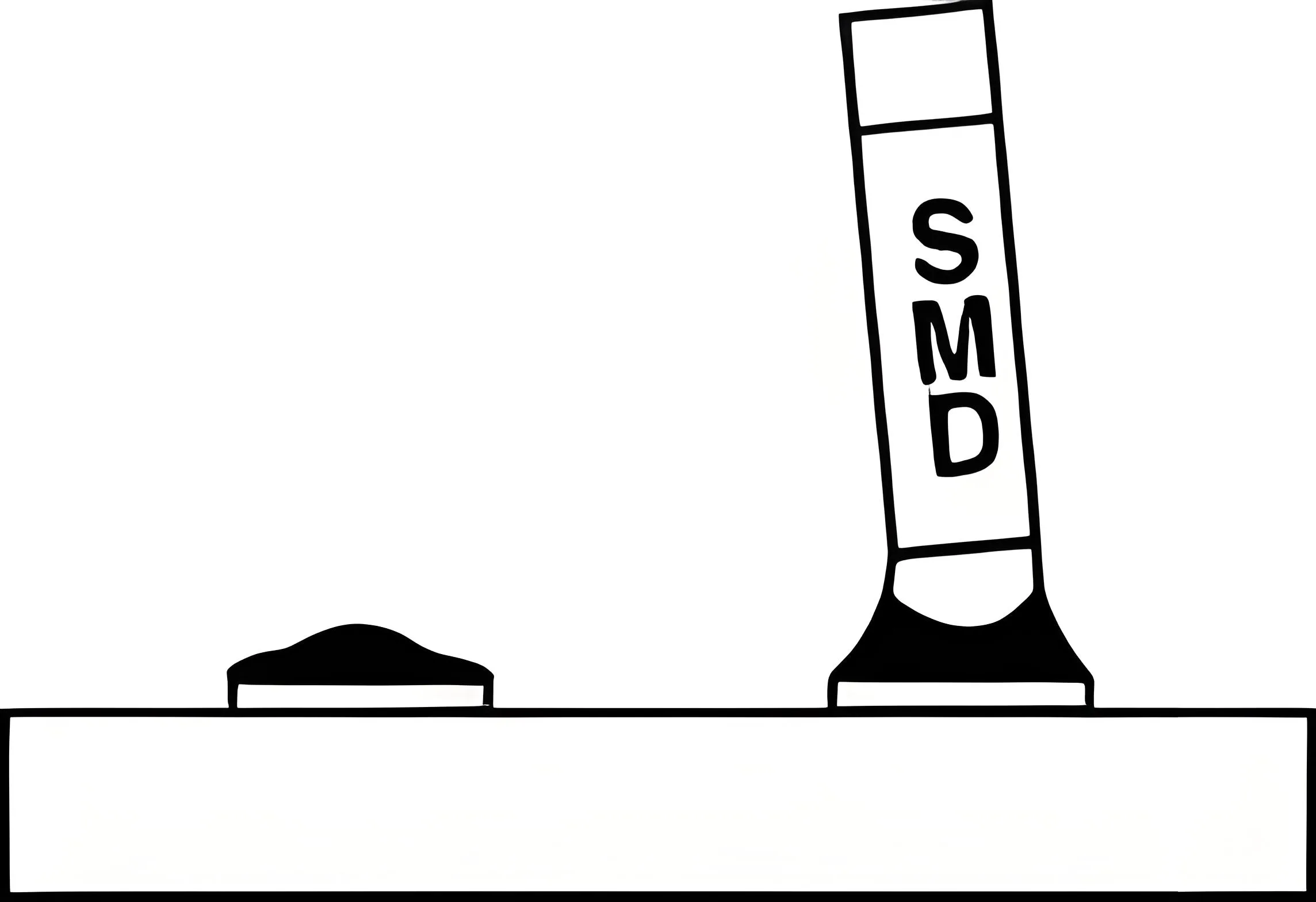
Le problème principal provient d'un déséquilibre de couple provoqué par des forces inégales sur les extrémités des composants.. Lorsque la pâte à souder à une extrémité fond en premier et génère des forces de mouillage, tandis que l'extrémité opposée reste infondue, le différentiel de tension superficielle tire le composant vers le haut, formant une pierre tombale. Selon modèles mécaniques, le tombstoning se produit lorsque le facteur d'équilibre Eb dépasse 1.
Mécanisme mécanique et paramètres clés du phénomène Manhattan
Analyse du modèle de force
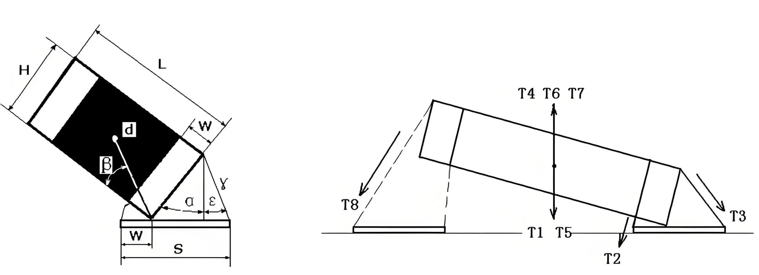
Les forces agissant sur un composant lors du brasage par refusion sont complexes et comprennent principalement les moments suivants:
-
Moments de résistance:
-
T1 = Gestion des cos(a+b) (gravité des composants)
-
T2 = γωcos(a/2) (tension superficielle de la soudure fondue au bas du composant)
-
T5 = Adcos(a+b) (force d'adhérence de la pâte à souder)
-
-
Moments de conduite:
-
T3 = γHsin(a+d) (tension superficielle au niveau du congé d'extrémité du composant)
-
T6 = Mvdcos(a+b) (force induite par les vibrations du convoyeur)
-
T7 = Lhρgdcos(a+b) (flottabilité maximale due à la génération de gaz dans la pâte à souder)
-
Facteur d’équilibre Eb = (T3 + T6 + T7) / (T1 + T2 + T5)
Quand Mib > 1, les moments de conduite dépassent les moments de résistance, provoquant inévitablement l'effet Manhattan.
Rôle critique de la tension superficielle
La pâte à souder fondue minimise la surface selon le principe de minimisation de l'énergie. Sa tension superficielle est définie par σ = (Fs – Fv) · n1, où Fs est l'énergie libre de surface, Fv est l'énergie libre de volume, et n1 est le nombre de molécules par unité de surface.
De l'équation de Laplace, la pression supplémentaire à la surface du liquide est: Pad = 2σH, où H = ½(1/R1 + 1/R2). Les différences de courbure de la soudure fondue aux extrémités des composants créent une pression supplémentaire inégale, conduisant à une tension superficielle non uniforme et déclenchant un tombstoning.
Analyse de 16 Facteurs clés influençant le phénomène Manhattan
Conception des PCB et facteurs matériels
-
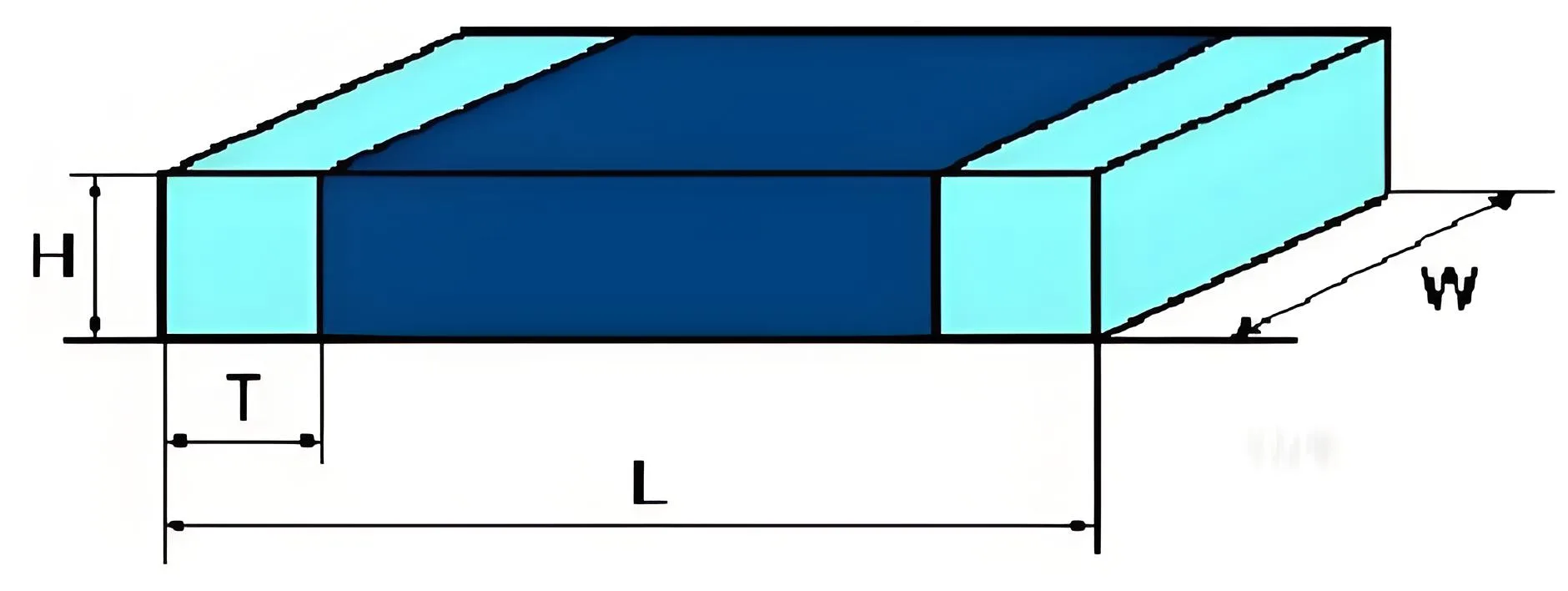
Conception de coussin asymétrique: Le non-respect des normes IPC-7351/IPC-SM-782 entraîne une capacité thermique inégale. Les dimensions recommandées des tampons doivent respecter strictement les normes; par ex., pour 0402 composants, longueur du tampon A = 1,50 mm, largeur B = 0,50 mm.
-
Inadéquation entre l'espacement des composants et des plots de circuit imprimé: Provoque des forces de mouillage déséquilibrées.
-
Variation de la capacité thermique des tampons: Les coussinets plus grands ont une capacité thermique plus élevée, chauffer plus lentement, et retarder la fusion de la soudure.
-
Substrat PCB Conductivité thermique: L'incidence est la plus élevée avec les substrats en papier époxy (≥8%), suivi de verre époxy (≈5%), et le plus bas avec de la céramique d'alumine (≤2%).
-
Volume de pâte à souder asymétrique: Une erreur d'impression ou une épaisseur incohérente entraîne des différences de capacité thermique.
-
Contamination ou oxydation de la couche de nickel ENIG: Entraîne une mauvaise mouillabilité et un temps de mouillage prolongé.
-
Revêtement HASL fin: Forme des couches IMC inférieures, force de mouillage insuffisante.
-
Variation de l'activité de la pâte à souder: Mauvaise uniformité du flux ou pré-volatilisation excessive.
Facteurs de processus et d'équipement SMT
-
Chauffage inégal aux extrémités des composants: Variation latérale de température du four de refusion ΔT > ±2 °C fait fondre une extrémité en premier.
-
Placement des composants mal alignés: >25% une différence dans le chevauchement des plots entre les composants et les PCB provoque un transfert de chaleur inégal.
-
Tombstoning dû au placement sans contact: Les composants qui ne sont pas entièrement en contact avec la pâte à souder entravent la conduction thermique.
-
Vol de soudure ou évents dans les vias adjacents: Réduit le volume de pâte à souder, modification de la capacité thermique.
-
Effet de mur de vent dans les fours de refusion: Une fréquence de ventilateur incorrecte crée des différences de température localisées.
-
Préchauffage insuffisant: Une température ou une durée de préchauffage inadéquate augmente ΔT.
-
Orientation incorrecte des composants: Ne parvient pas à assurer l’entrée simultanée des deux extrémités dans la zone de refusion.
-
Utilisation incorrecte de l'atmosphère N2: Une prévention excessive de l’oxydation accélère le mouillage initial, réduire la fenêtre de réglage ΔT.
Stratégie globale de prévention et de solution au phénomène de Manhattan
Optimisation de la conception des pads – Adhérer aux normes IPC
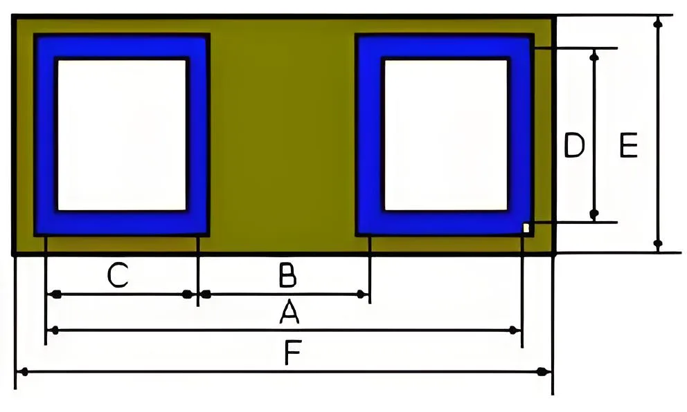
Le strict respect des normes IPC-7351B pour la conception des supports est fondamental. Dimensions recommandées des tampons (en mm) sont:
| Type de composant | Longueur du tampon (UN) | Largeur du tampon (B) | Espacement des tampons (C) | Longueur du tampon sous-composant (D) |
|---|---|---|---|---|
| 0201 | 0.75 | 0.23 | 0.23 | 0.31 |
| 0402 | 1.50 | 0.50 | 0.50 | 0.60 |
| 0603 | 2.10 | 0.90 | 0.60 | 0.90 |
| 0805 | 2.60 | 1.20 | 0.70 | 1.30 |
Assurer la symétrie des tampons; La longueur du patin sous le composant doit dépasser la largeur de l'extrémité métallique pour améliorer le moment anti-chute T2.
Affiner les processus d'impression et de placement
-
Contrôle de l'impression de la pâte à souder: Utiliser le SPI 3D pour inspecter l'épaisseur et la surface de la pâte, assurer la différence de volume entre les extrémités <10%. Maintenir l'épaisseur entre 100 et 130 μm, avec nettoyage régulier du pochoir et test de tension.
-
Amélioration de la précision du placement: Utilisez des placers haute vitesse Siemens série SX avec étalonnage laser 3D pour une précision de placement de ± 25 μm, assurant un contact uniforme entre les extrémités des composants et la pâte à souder.
-
Optimisation de l'orientation des composants: Conception avec axe long du composant perpendiculaire à la ligne limite de refusion, permettant l'entrée simultanée des deux extrémités dans la zone de fusion pour une fusion synchronisée.
Contrôle précis du profil de soudage par refusion
-
Préchauffage adéquat: Préchauffer à 150-180°C pendant 60-120 secondes, réduisant ΔT entre les extrémités à ±2°C près.
-
Montée en puissance contrôlée: Maintenir la pente entre 1,0 et 2,0 °C/s pour éviter les chocs thermiques.
-
Température maximale: 235–245°C pour une soudure sans plomb, avec un temps au-dessus du liquidus de 45 à 75 secondes.
-
Uniformité de la température du four: Surveiller et calibrer régulièrement la température du four, assurer la variation latérale des planches <±2°C.
Alt: Comparaison entre optimisé et. profils de brasage par refusion standard mettant en évidence les différences de préchauffage et de température maximale.
Mises à niveau des matériaux et des équipements
-
Sélection de pâte à souder: Utilisez des pâtes non eutectiques à double point de fusion pour prolonger le temps de mouillage complet et réduire ΔT. Les pâtes à haute viscosité offrent une résistance mécanique pour contrer la tension superficielle.
-
Mise à niveau de l'équipement: Mettre en œuvre des systèmes de refusion ERSA avec protection N2 à 16 zones, contrôler les fluctuations de température maximale à ± 1,5 °C.
-
Amélioration du système AOI: Déployez une inspection optique automatique avec une précision de 0,02 mm² pour une détection des chutes en temps réel.
Système de prévention et de traçabilité basé sur les données
Établir un système de traçabilité numérique complet du processus utilisant le MES pour surveiller 120+ paramètres clés du processus, enregistrement des données par carte pour la position de placement et la température de soudure. Lorsque les taux de désactivation dépassent les seuils (par ex., >1.5% pour 0402 composants), identifier rapidement les équipements et les opérateurs spécifiques pour une correction ciblée.
Mettre en œuvre un contrôle statistique du processus SPC pour surveiller les paramètres clés tels que le facteur d'équilibre Eb, ΔT, et décalage de placement en temps réel, créer des mécanismes d’alerte précoce pour une prévention proactive.
Conclusion: Stratégie intégrée pour 99.9% Rendement au premier passage
Le phénomène Manhattan est un problème multifactoriel dans la fabrication SMT nécessitant une prévention systématique:
-
Concevoir d'abord: Suivre strictement les normes IPC-7351, optimiser la conception des pads, et assurer l'équilibre thermique.
-
Précision du processus: Impression de contrôle, placement, et étapes de refusion pour minimiser les différences de ΔT et de temps de mouillage.
-
Matériaux de haute qualité: Sélectionnez des pâtes à braser avec une activité appropriée et une répartition uniforme du flux.
-
Équipement stable: Garantir que l'uniformité de la température du four et la précision du placement répondent aux normes.
-
Approche basée sur les données: Mettre en œuvre la traçabilité complète du processus et le SPC pour une prévention tournée vers l’avenir.
Grâce à ces mesures, Fabricants de PCBA peut réduire les taux de défauts de Manhattan ci-dessous 0.1%, atteindre 99.9% rendement de premier passage, et répondez aux exigences de fiabilité extrêmes des PCB haut de gamme pour les serveurs d'IA et l'électronique automobile. Dans cette nouvelle phase de PCB transition de valeur de l'industrie, vaincre le phénomène Manhattan n’est pas seulement un défi technique mais une étape essentielle pour renforcer la compétitivité.
Agissez dès aujourd’hui: Pour une prise en charge de la conception de plots de composants conformes à la norme IPC ou des devis de traitement PCBA, contactez notre équipe technique pour des solutions de bout en bout, de la conception de PCB à la production, Assemblage PCBA, et PECVD protection.
