Quand Amazon $100 milliard 2025 Capex entre en collision avec Openai “Stargate,” Une révolution matérielle dirigée par l'IA est de remodeler la chaîne d'approvisionnement de l'électronique - où les modules optiques et PCB servir de moteurs de base.
Course des armes informatiques mondiales: Paysage des dépenses en capital
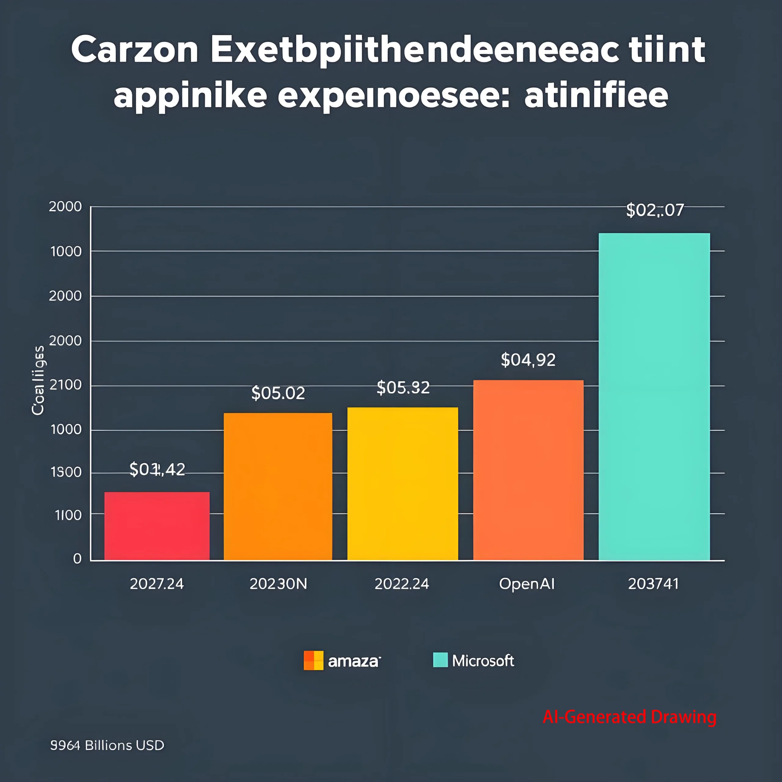
Géants à l'étranger: $100B + Capex Surge
-
Amazone: $75B Capex dans 2024, projeté >$100B dans 2025 (à l'origine du nuage)
-
Google: $17.2B Q1 2025 capex (+44% En glissement annuel), $75B Plan de l'année complète
-
Microsoft: $16.7B Q1 2025 (+53% En glissement annuel), accélérer les investissements dans le cloud AI
-
Méta: Capex élevé à 60-65 milliards de dollars (LLM R&D + matériel personnalisé)
Statistique clé: Haut 4 CSPS ’ 2025 Capex total dépasse 300 milliards de dollars, croissance >35% En glissement annuel.
Joueurs émergents: Nouveaux entrants agressifs
-
Openai: “Stargate” Projet de supercalculateur (>$100B Coût estimé)
-
Tesla / Apple: Faire monter les investissements matériels pour en interne AI chips
-
Changement de l'industrie: Haut 4 Le partage CSPS CAPEX tombe de 59% (2023) à <50% (2025)
“Alors qu'Openai construit des supercalculateurs et Tesla développe des puces Dojo, Les limites traditionnelles du centre de données s'effondrent.”
Guerres de puce AI: GPU VS. Bataille ASIC
GPU: Fondation de l'informatique Empire
-
Dominance: Poignées >90% de la formation du modèle IA
-
Métrique de performance:
Compute Density (TFLOPS/mm²) = Transistor Count × Frequency × Core Efficiency -
L'avance de Nvidia: Bande passante H100 3Tb / s, Vitesse nvlink 900GB / s
ASIC: Révolution des puces personnalisées
-
Efficacité énergétique: 40-60% inférieur Power vs. GPU à la même calcul
-
Formule de retour sur investissement:
ROI (months) = (Power Savings × Scale) / (R&D Cost ÷ Lifespan) -
Projection de croissance: Prévisions Marvell 2028 Vous avez un marché ASIC >$40B (47% TCAC)
Révolution architecturale: Grappes hyper-nœuds
-
Cluster HWJ 384-nœud:
Theoretical Compute = Single-Chip Power × 384 × Interconnect Efficiency (≈1.7×NVL72) -
Limitation GB 200: Interconnexion en cuivre max 72 cartes, Optical Breaks Topology Barrières
PCB / modules optiques: Bénéficiaires de base de calcul Boom
PCB du serveur AI: Révolution de la couche & Matériel Innovation
| Type de serveur | Couches de PCB | Taux de données | Prime de prix |
|---|---|---|---|
| Traditionnel | 6-8 | ≤ 56 Gops | Base de base |
| Serveur GPU | 12-16 | 112Gbit/s | +300% |
| Nœud ASIC | 20+ | 224Gbit/s | +700% |
Percée:
-
Cuivre lourd: 3poignées d'aluminium oz >1000UN actuel
-
Matériaux hybrides: Megatron ™ 8 Df ≤0,0015 (@ 112 GHz)
Modules optiques: CPO VS. LPO Tech Divide
-
Surtension de la demande: >5,000 modules par cluster ASIC
-
Chemins technologiques:
-
LPO (Entraînement linéaire): Pouvoir ↓ 50%, latence <2ns
-
CPO (Optique co-emballée): Densité ↑ 5 ×, coût ↓ 30%
-
-
Dimensionnement du marché:
Optical Market = AI Chip Volume × Interconnect Ratio × Penetration Rate
Prévisions clés: 1.6T adoption du module à atteindre 25% par 2025 (Revêtement léger)
Ascension de la Chine: Percées de localisation
Infrastructure informatique axée sur les politiques
-
Poyeuses nationales: 70+ centres de données en construction, 600K + nouveaux racks
-
Calculer la cible: 1,037.3 Eflops par 2025 (43% Croissance en glissement annuel)
Localisation matérielle: PCB / progrès optique
| Segment | Taux de localisation | Dirigeants | Innovations |
|---|---|---|---|
| PCB à grande vitesse | 35% | UGPCB / Deepkin / Tech | 112GBPS Perte ultra-faible |
| Modules optiques | 60%+ | Innolight / Eoptolink | 1.6TRAPPOSSION DE MASSE CPO |
| Substrats IC | <15% | UGPCB / Sinxing | 2.5D emballage D TSV |
Impact tarifaire: PCB haut de gamme Coûts de réinstallation >30%, renforcement des chaînes d'approvisionnement locales
Focus d'investissement: Analyse des leaders
Positionnement des fabricants de PCB
-
Ucp : Core Nvidia HGX Substrat Fournisseur, rendement >95%
-
Et la technologie: Matériaux de qualité m7 nvidia certifiés, partager la montée
-
Deepkin: 3D substrat capacité ↑ 300%
Paysage des vendeurs de modules optiques
| Fournisseur | Technologie de base | 800Statut g | 1.6T progressive |
|---|---|---|---|
| Innolight | LPO + Photonique en silicium | Production de masse | Échantillonnage |
| Eoptolink | Intégration CPO | Petit lot | Scène de laboratoire |
| Cambridge Tech | Linbo à couches minces | Essai | - |
Équipement & Champions matériels
-
Précision Nikon: Lithographie d'imagerie directe ≤2μm
-
Brouillard: Film de blindage ultra-mince ≤5μm
-
Wazam Nouveaux matériaux: DK / df bas Mégatron 8
2025-2028 Feuille de route technologique
-
Échelle de la couche PCB:
Avg AI Server Layers = 12 + 0.5×(Annual Compute Growth)→ 24L par 2028 -
Intégration optique:
-
Adoption du CPO >15% par 2025
-
Optique embarquée (Obo) production de 2027
-
-
Innovations thermiques:
-
Résistance thermique PCB refroidie par liquide <0.1° C / W
-
Conductivité des matériaux à changement de phase >20Avec mk
-
Aperçu de l'industrie: “Lorsque la demande de calcul double trimestriel, Ce n'est qu'en gravissant des chemins lumineux sur les PCB et en construisant des villes en silicium 3D que nous pouvons conduire le tsunami AI.”