
Introduction au 24 Layers Communication Backplane PCB
Le 24 Layers Communication Backplane PCB is a high-performance circuit imprimé designed for complex communication systems. It is engineered to provide robust connectivity and reliable signal transmission, making it ideal for advanced telecommunication applications.
Qu'est-ce qu'un 24 Layers Communication Backplane PCB?
UN 24 Layers Communication Backplane PCB refers to a multilayered printed circuit board that has been specifically designed with 24 layers of conductive material separated by dielectric layers. This structure allows for high-density interconnectivity while maintaining signal integrity and minimizing interference.
Exigences de conception
The design requirements for a 24 Layers Communication Backplane PCB are stringent due to its application in critical communication systems. Key design considerations include:
- Matériel: Panasonic M6, known for its excellent thermal and electrical properties.
- Nombre de couches: 24 layers to accommodate complex routing needs.
- Couleur: Blue/White for easy identification and aesthetic appeal.
- Épaisseur finie: 2.0mm to ensure structural integrity without being overly bulky.
- Épaisseur du cuivre: 1OZ to provide adequate conductivity.
- Traitement de surface: Immersion de l'or pour améliorer la soudabilité et la résistance à la corrosion.
Comment ça marche?
Le 24 Layers Communication Backplane PCB works by using multiple layers of copper traces separated by dielectric materials. These layers are interconnected through plated through-holes (PTH) or vias, allowing signals to travel between different layers. The immersion gold surface treatment ensures that the copper traces remain conductive and resistant to oxidation.
Applications
The primary application of the 24 Layers Communication Backplane PCB is in communication backplanes where high-speed data transmission and reliable connectivity are crucial. Ces PCB are used in:
- Telecom infrastructure
- Centres de données
- High-frequency communication devices
- Networking equipment
Classification
En fonction de ses fonctionnalités et applications, le 24 Layers Communication Backplane PCB can be classified as a high-multilayer PCB. This classification highlights its capability to handle complex and dense circuit designs required for modern communication systems.
Composition des matériaux
Le noyau matériel used in the 24 Layers Communication Backplane PCB is Panasonic M6, un matériau stratifié haute performance connu pour son excellent mécanique, thermique, et propriétés électriques. This material ensures that the PCB can withstand the demands of high-speed communication applications.
Caractéristiques de performance
The performance characteristics of the 24 Layers Communication Backplane PCB include:
- High signal integrity
- Low signal loss
- Gestion thermique supérieure
- Enhanced mechanical strength
- Reliable long-term stability
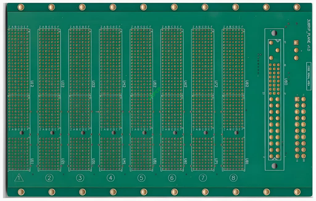
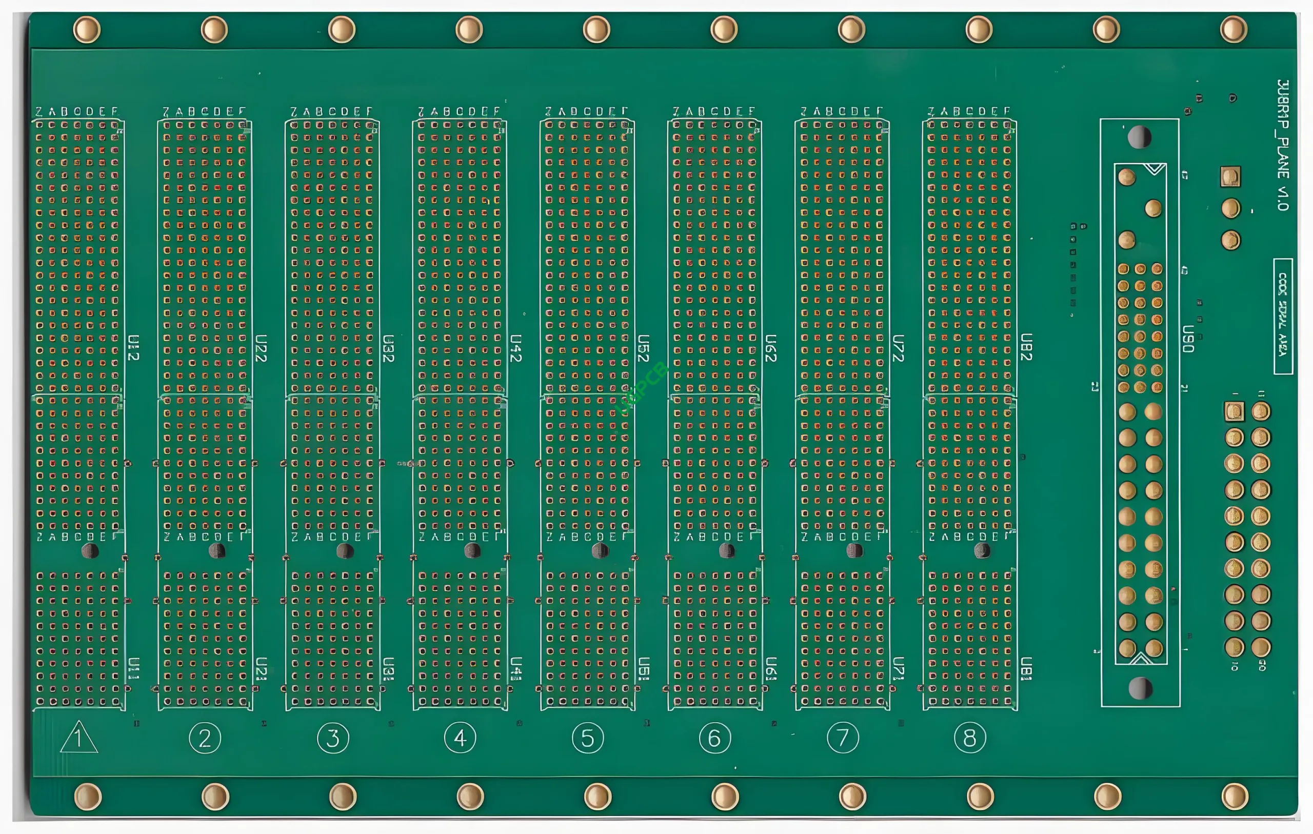
Détails structurels
The structural details of the 24 Layers Communication Backplane PCB are as follows:
- Nombre de couches: 24 couches
- Épaisseur finie: 2.0mm
- Épaisseur du cuivre: 1once
- Largeur de trace minimale: 6mil (0.15mm)
- Minimum Space Between Traces: 6mil (0.15mm)
- Traitement de surface: Immersion Or
Caractéristiques et avantages
The key features and benefits of the 24 Layers Communication Backplane PCB include:
- Interconnectivité à haute densité
- Excellente intégrité du signal
- Construction mécanique robuste
- Performance fiable à long terme
- Options de couleurs esthétiques (Bleu/Blanc)
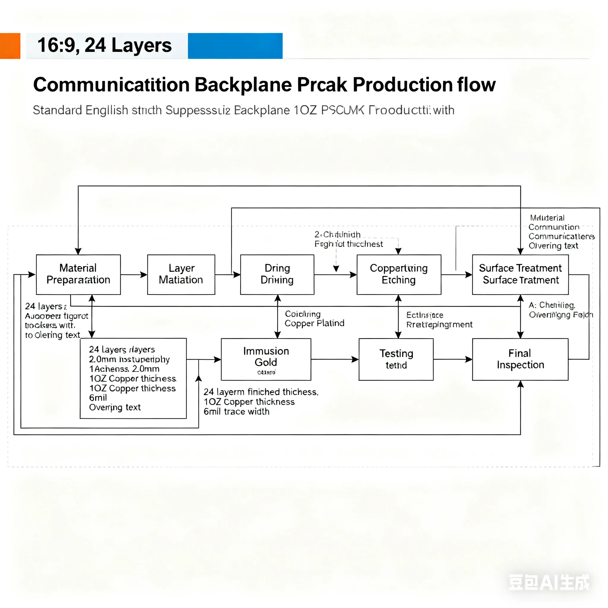
Processus de production
The production process of the 24 Layers Communication Backplane PCB involves several steps, y compris:
- Sélection des matériaux: Choosing high-quality Panasonic M6 material.
- Empilement de calques: Arrangeant le 24 couches avec précision.
- Gravure: Supprimer l'excès de cuivre pour former les modèles de trace souhaités.
- Placage: Appliquer un traitement de surface en or d'immersion.
- Assemblée: Incorporer les PTH et les vias pour les interconnexions de couche.
- Essai: Assurer que le PCB répond à toutes les spécifications de performance.
Cas d'utilisation

Le 24 Layers Communication Backplane PCB is used in various scenarios, tel que:
- High-speed data transmission networks
- Telecommunication infrastructure projects
- Advanced networking equipment
- Data center applications requiring high bandwidth
En résumé, le 24 Layers Communication Backplane PCB is a sophisticated and reliable component designed to meet the demanding requirements of modern communication systems. Its high-density design, excellent performance characteristics, and robust construction make it an essential part of any advanced telecommunication setup.


