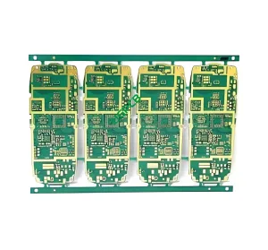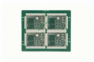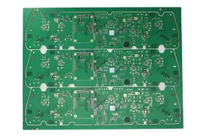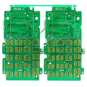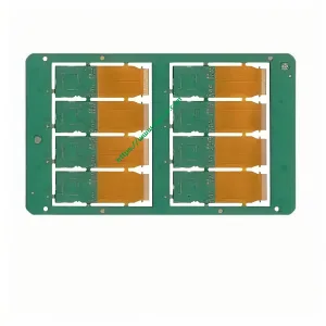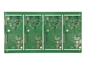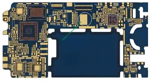
Introduction to the 4L 1+N+1 HDI Wifi Module Product Overview
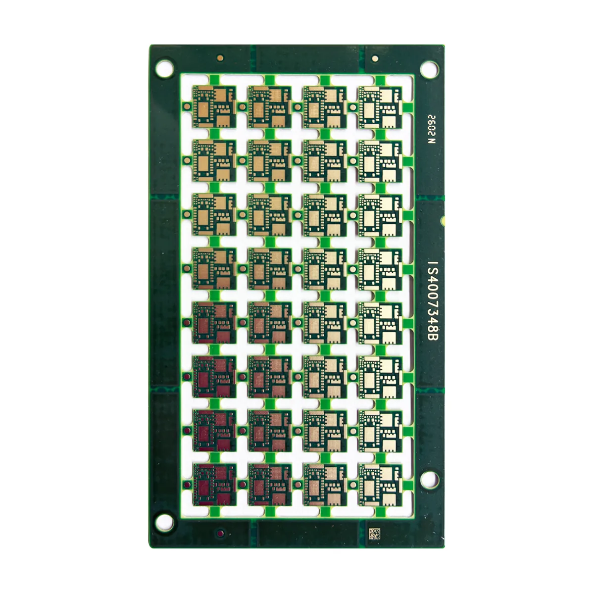
The 4L 1+N+1 HDI Wifi Module is a cutting-edge electronic module designed for high-density interconnect applications. This module utilizes advanced technology to ensure reliable and efficient performance in various electronic devices.
Définition
A High-Density Interconnect (IDH) module refers to a circuit imprimé (PCB) that features higher wiring density than traditional PCBs, enabling more compact and complex designs. Le “4L 1+N+1” designation indicates a four-layer structure with specific layer configurations.
Exigences de conception
The 4L 1+N+1 HDI Wifi Module is meticulously designed to meet stringent requirements:
- Calques: Four layers with a specific stack-up of 1+N+1.
- Matériel: Made from high-quality Matériau FR-4.
- Épaisseur: The overall finished thickness of the module is 1.0mm.
- Épaisseur du cuivre: Features inner copper layers at 1OZ and outer layers at 0.5OZ.
- Traitement de surface: Incorporates immersion gold and Organic Solderability Preservatives (OSP) for enhanced durability and solderability.
- Trace / espace min: Supports minimal trace and space widths of 4mil.
- Trou minimum: Accommodates mechanical holes as small as 0.2mm and laser holes as fine as 0.1mm.
Principe de fonctionnement
The 4L 1+N+1 HDI Wifi Module operates by utilizing high-frequency signals transmitted via its integrated antenna to connect to Wi-Fi networks. The module’s HDI design allows for efficient signal routing and minimal interference, ensuring robust and stable connectivity.
Applications
This versatile module is suitable for a wide range of applications including but not limited to:
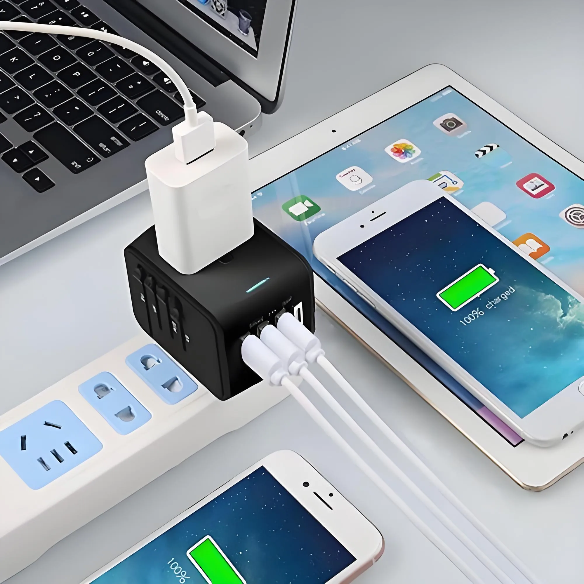 Electronique grand public: Smartphones, comprimés, appareils intelligents pour la maison.
- Équipement industriel: Automation systems, control panels.
- Appareils de communication: Routeurs, access points, set-top boxes.
Classification
The module falls under the category of high-density interconnect printed circuit boards, specifically tailored for applications requiring compact size and high performance.
Composition des matériaux
Constructed from FR-4, un stratifié époxy renforcé de verre ignifuge, the module ensures excellent thermal and electrical properties. The copper layers provide conductive pathways essential for signal transmission.
Caractéristiques de performance
- Intégrité du signal: Maintains high signal integrity due to minimized trace lengths and optimized layer stack-up.
- Gestion thermique: Efficient heat dissipation thanks to the material properties of FR-4 and the design architecture.
- Durabilité: Enhanced durability with surface treatments like immersion gold and OSP, protecting against oxidation and improving solder joint reliability.
Caractéristiques structurelles
- Quadrilateral Foramen: A specialized process involving the creation of square-shaped holes, allowing for intricate component placement and routing.
- Empilement des couches: The unique 1+N+1 layer arrangement optimizes space utilization and signal integrity.
Processus de production
The manufacturing process involves several key steps:
- Préparation des matériaux: Cutting and preparing the FR-4 substrate.
- Laminage de cuivre: Applying copper layers on both sides and inner layers as per design.
- Gravure: Removing excess copper to form the desired circuit patterns.
- Alignement des calques: Stacking and aligning the layers accurately.
- Collage: Utiliser la chaleur et la pression pour lier les couches ensemble.
- Traitement de surface: Applying immersion gold and OSP finishes.
- Contrôle de qualité: Conducting thorough inspections and tests to ensure product quality

Scénarios de cas d'utilisation
Electronique grand public
In smartphones and tablets, the 4L 1+N+1 HDI Wifi Module ensures reliable wireless connectivity while maintaining a slim profile.
Équipement industriel
Pour les systèmes d'automatisation, the module provides dependable communication links in harsh industrial environments.
Appareils de communication
In routers and access points, the module enhances network performance with its superior signal handling capabilities.
By adhering to these design and production standards, the 4L 1+N+1 HDI Wifi Module delivers exceptional performance and reliability, making it an ideal choice for modern electronic applications.