

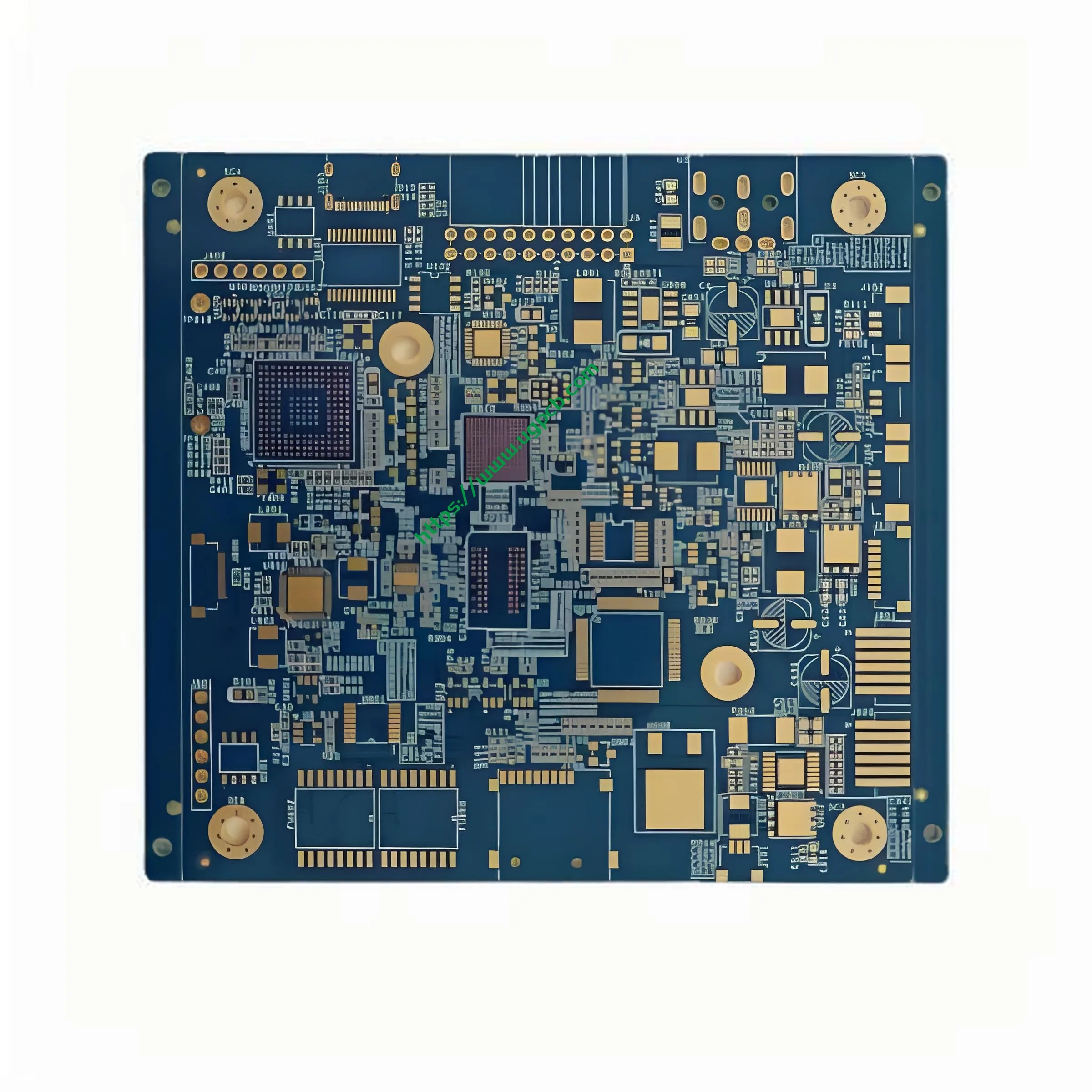
What is a 6L 1+N+1 HDI PCB?
A 6L 1+N+1 HDI PCB stands for a six-layer High Density Interconnect (IDH) circuit imprimé, featuring one core layer flanked by N signal layers and another core layer. This configuration allows for high density interconnections, making it suitable for advanced electronic applications. Le “1+N + 1” designation refers to the arrangement of the core layers and signal layers.
Exigences de conception
The design of a 6L 1+N+1 HDI PCB requires careful consideration of several factors:
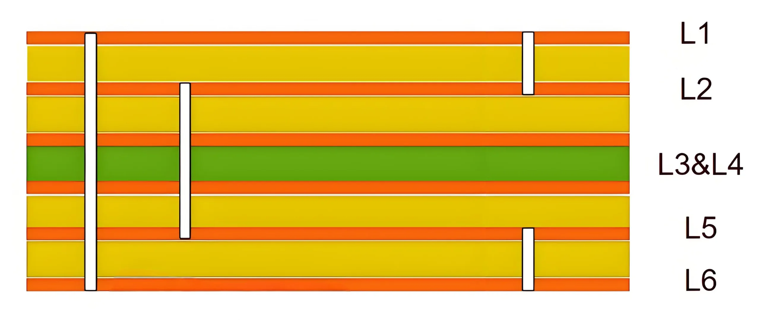
- Empilement de calques: Proper alignment of the core and signal layers to ensure optimal electrical performance.
- Trace et espace: Minimal trace width and space of 3mil/3mil to accommodate fine features.
- Hole Sizes: Mechanical holes as small as 0.2mm and laser holes down to 0.1mm for precise component placement.
- Épaisseur du cuivre: Varied copper thickness with inner layers at 1OZ and outer layers at 0.5OZ to balance conductivity and flexibility.
Comment ça marche?
The functionality of a 6L 1+N+1 PCB HDI relies on its multilayer structure and the use of high-density interconnects. Each layer serves a specific purpose:
- Core Layers: Provide structural integrity and act as the foundation for signal layers.
- Signal Layers: Carry electrical signals between components.
- Traitement de surface en or par immersion: Ensures excellent solderability and long-term reliability by preventing oxidation.
Applications et classifications
Ces PCB are primarily used in intelligent digital products where compact size and high performance are crucial. They can be classified based on their complexity and the number of layers, with the 6L 1+N+1 configuration being highly versatile for various applications.
Matériaux et performances
Constructed from FR-4 (ITEQ), these PCBs offer excellent thermal stability and mechanical strength. The green/white color scheme aids in visual inspection and troubleshooting. The finished thickness of 1.0mm provides a robust yet flexible board suitable for intricate designs.
Structure et caractéristiques
The unique structure of a 6L 1+N+1 HDI PCB includes:
- Six couches: One core layer, N Couches de signal, and another core layer.
- High Density Interconnects: Allow for complex routing and minimal space usage.
- Surface dorée par immersion: Enhances conductivity and protects against corrosion.
Processus de production
The manufacturing process involves several sophisticated steps:
- Préparation des matériaux: Selecting high-quality FR-4 substrate and copper foils.
- Empilement de calques: Arranging the layers in a precise order to achieve the desired “1+N + 1” configuration.
- Collage: Utiliser la chaleur et la pression pour lier les couches ensemble.
- Gravure: Application d'un agent de gravure pour éliminer l'excès de cuivre, ne laissant que les chemins conducteurs souhaités.
- Placage: Adding a thin layer of metal to improve conductivity and solderability.
- Traitement de surface: Applying immersion gold to protect against oxidation and enhance solderability.
- Contrôle de qualité: Effectuer des inspections et des tests approfondis pour garantir que chaque carte répond à des normes de qualité strictes.

Des cas d'utilisation et des scénarios
6L 1+N+1 HDI PCBs are ideal for use in intelligent digital products where miniaturization and high performance are critical. Les applications courantes incluent:
- Smartphones: Permettre des conceptions plus fines sans compromettre la fonctionnalité ou les performances.
- Comprimés: Fournir une connectivité fiable pour le transfert et le traitement des données à haut débit.
- Appareils portables: Prise en charge des conceptions compactes tout en conservant des performances et une durabilité robustes.


