
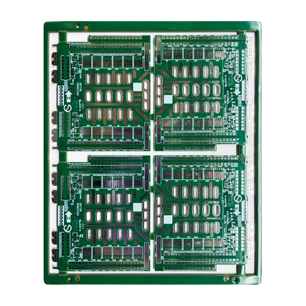
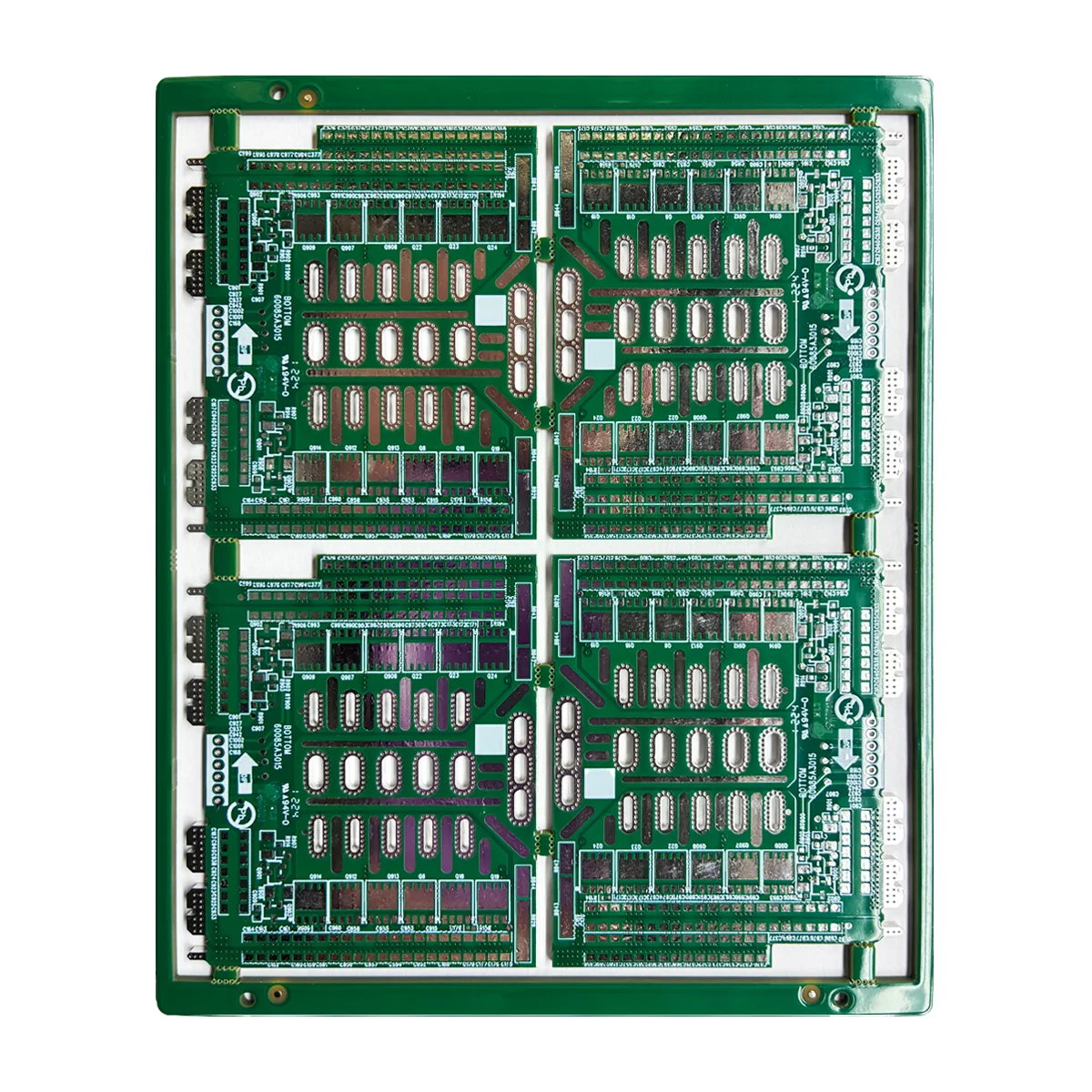
PCB rigide à 8 couches haute fiabilité Présentation du produit & Définition
Au royaume du haut débit, conception électronique haute densité, PCB multicouches (Cartes de circuits imprimés) sont indispensables. UGPCB 8-PCB rigide en couche, construit avec un important 2.0mm épaisseur du panneau et 3Feuille de cuivre lourde OZ, est conçu pour résister aux environnements électriques et physiques exigeants. Il sert non seulement de base à la connectivité électrique, mais aussi de composant essentiel garantissant la stabilité de l'appareil et une fiabilité accrue du produit.. Pour les applications dans les contrôles industriels, systèmes électriques, ou électronique automobile, cette carte de haute spécification est la solution optimale pour les applications complexes, des conceptions performantes.
Spécifications de base
-
Nombre de couches: 8-PCB rigide en couche
-
Épaisseur du panneau fini: 2.0mm ±10%
-
Matériau de base: FR-4, Température de transition du verre (Tg) ≥ 170°C
-
Finition de surface: Nivellement de soudure à air chaud sans plomb (HASL-LF)
-
Poids du cuivre: 3 onces par pied carré (≈105μm) pour les couches intérieures et extérieures
-
Masque de soudure & Écran à soigneux: Masque de soudure LPI vert, Légende de la sérigraphie blanche
Considérations critiques de conception
Lors de la conception avec ce PCB haute spécification, les ingénieurs doivent donner la priorité:
-
Gestion thermique: Tirer parti de la capacité de transport de courant élevée de 3Cuivre lourd OZ pour optimiser la puissance et les plans de masse, réduisant l'impédance et l'échauffement. Utilisez la simulation thermique en conjonction avec la résistance élevée à la chaleur de Matériau FR-4 TG170.
-
Contrôle de l'impédance & Intégrité du signal: L'empilement à 8 couches permet une séparation efficace du signal, pouvoir, et couches de sol. Calcul précis et contrôle de l'impédance de trace (par ex., 50Ω asymétrique, 100différentiel Ω) est essentiel pour minimiser la réflexion et la diaphonie.
-
Mécanique & Fiabilité électrique: Le 2.0panneau de mm d'épaisseur améliore la rigidité globale, adapté aux applications avec vibrations ou contraintes d'insertion. Pour les nœuds haute tension ou courant élevé, ajuster la largeur de trace et le jeu en fonction Normes IPC-2221 et le 3Poids en cuivre OZ pour garantir des marges de sécurité.
-
DFM (Conception de la fabrication): Collaborer dès le début avec l’équipe d’ingénierie de l’UGPCB pour répondre aux exigences spécifiques de PCB en cuivre lourd et PCB à panneau épais traitement, tels que les paramètres de perçage et l'uniformité du placage, garantir un processus de fabrication à haut rendement.
Comment ça marche & Structure
Un 8-couche PCB est fabriqué en stratifiant plusieurs couches conductrices en une seule unité à l'aide de processus précis, notamment l'imagerie de la couche interne, laminage, forage, et placage. Les connexions électriques entre les couches sont établies via trous traversants plaqués (PTH), vias aveugles, ou vias enterrés. Un exemple typique de stack-up est:
Couche supérieure (Signal) — Préimprégné — L2 (Sol) — Noyau — L3 (Signal) — Noyau — L4 (Pouvoir) — Noyau — L5 (Signal) — Préimprégné — Couche inférieure (Signal)
Ce “sandwich” la structure isole efficacement les signaux à grande vitesse, fournit des plans de référence solides, et assure une distribution efficace de l'énergie.
Performance & Caractéristiques clés
-
Performance électrique supérieure: 3Cuivre lourd OZ offre une résistance de conducteur extrêmement faible et une excellente capacité de transport de courant (plus de 3 fois celui du cuivre standard de 1 OZ), réduisant la perte de puissance et la chute de tension.
-
Fiabilité thermique exceptionnelle: Matériau FR-4 TG170 à haute Tg résiste à des températures de fonctionnement et de soudage plus élevées. Combiné avec la conductivité thermique du cuivre lourd, il améliore considérablement la fiabilité à long terme dans les environnements à haute température.
-
Stabilité mécanique améliorée: Le 2.0panneau de mm d'épaisseur combiné au FR-4 rigide, il offre une résistance supérieure à la flexion et aux vibrations, idéal pour les conditions de fonctionnement difficiles.
-
Fiabilité élevée des joints de soudure: Le Finition de surface HASL-LF fournit un appartement, surface de tampon coplanaire avec une excellente soudabilité et une durée de conservation prolongée, conforme aux directives RoHS.
-
Interconnexion à haute densité (IDH) Capacité: La conception à 8 couches offre un espace de routage suffisant pour les circuits complexes, facilitant la miniaturisation des appareils et l’intégration fonctionnelle.
Aperçu du processus de production
Revue technique → Découpe de matériaux (FR-4TG170) → Imagerie de la couche interne & Gravure (3once) → Traitement à l'oxyde & Stratification → Perçage Mécanique & Placage de cuivre → Modelage de la couche externe & Placage (à 3OZ) → Application du masque de soudure (IPV vert) & Écran à soigneux (Blanc) → Finition de surface HASL sans plomb → Tests électriques & Inspection finale (selon les normes IPC)
Chaque étape intègre des points de contrôle de qualité rigoureux pour garantir que chaque PCB multicouche haute fiabilité répond aux spécifications exactes du client.
Applications principales & Cas d'utilisation
Ce PCB est conçu pour une puissance élevée, applications à haute stabilité:
-
Systèmes de contrôle industriels: Automates, entraînements à moteur, et alimentations industrielles nécessitant PCB en cuivre lourd pour courant élevé.
-
Énergie renouvelable & Systèmes électriques: Onduleurs solaires, Systèmes UPS, et modules de recharge pour véhicules électriques reposant sur une capacité de courant et une endurance thermique élevées.
-
Électronique automobile: Chargeurs embarqués (Obc), Systèmes de gestion de batterie (Bms), et convertisseurs DC-DC, où PCB à haute Tg sont essentiels pour les températures sous le capot.
-
Infrastructures de télécommunications: Amplificateurs de puissance de station de base et systèmes d'alimentation de secours de réseau.
-
Test haut de gamme & Équipement de mesure: Instruments nécessitant une alimentation stable et des performances à faible bruit.
Classement du produit (Selon les normes IPC)
-
Par nombre de couches: PCB multicouche (>4 couches), spécifiquement un 8-carte de circuit imprimé de couche.
-
Par rigidité: PCB rigide.
-
Par matériau de base: Carte FR-4, sous-ensemble: PCB à haute Tg (Tg ≥ 170°C).
-
Par processus spécial: PCB en cuivre lourd (pour IPC-2152), PCB à panneau épais.
-
Par classe d'application: Convient pour Classe CIB 2 (Produits électroniques à service dédié) et Classe 3 (Produits électroniques haute fiabilité) applications, y compris PCB de qualité industrielle, PCB électronique de puissance, et PCB de qualité automobile.


