
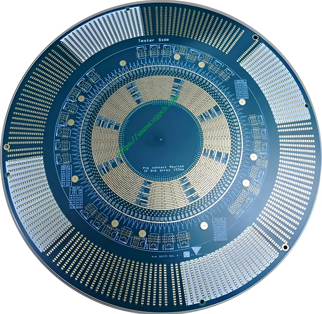
ATE Test Chip PCB Overview
The ATE test chip PCB is a specialized circuit imprimé designed for use in automated test equipment (A MANGÉ) systems for testing semiconductor chips. Ce PCB plays a crucial role in ensuring the quality and reliability of chips before they are integrated into electronic devices. Below is a detailed introduction to the ATE test chip PCB, couvrant ses informations générales, classification, matériels, performance, structure, caractéristiques, processus de production, et scénarios d'application.
Classification
ATE test chip PCBs are classified based on their layer count, composition des matériaux, et exigences de demande spécifiques. Le modèle introduit ici, ATE test chip PCB, is a 12-layer PCB, indicating its complexity and ability to handle intricate testing scenarios.
Composition des matériaux
The ATE test chip PCB is constructed using isola 370hr material, a high-performance, high-reliability substrate known for its excellent electrical and thermal properties. This material ensures the PCB’s ability to withstand the demanding test conditions and provide stable performance.
Caractéristiques de performance
The ATE test chip PCB excels in several performance areas, y compris une capacité de chargement à courant élevé, faible perte de signal, et excellente gestion thermique. The use of 2OZ copper thickness for inner layers and 1OZ for outer layers enhances its electrical conductivity and thermal dissipation capabilities. En plus, the immersion gold (5U) surface finish provides superior corrosion resistance and solderability, ensuring reliable connections during testing.
Conception structurelle
Structurellement, the ATE test chip PCB features a board thickness of 3.0mm, providing a robust foundation for the complex circuitry and composants. The green color not only adds a visual distinction but also aids in inspection and troubleshooting processes.
Caractéristiques distinctives
The ATE test chip PCB stands out with its unique features, including its high layer count, advanced material composition, and immersion gold surface finish. Ces fonctionnalités, combined with its precise design and manufacturing processes, make it an ideal choice for ATE chip testing applications.
Processus de production
The production of ATE test chip PCBs involves a series of sophisticated steps:
- Préparation des matériaux: The isola 370hr substrate is prepared and cut to the required dimensions.
- Laminage de cuivre: La feuille de cuivre est laminée au substrat, with specific attention to the inner layer 2OZ and outer layer 1OZ thickness requirements.
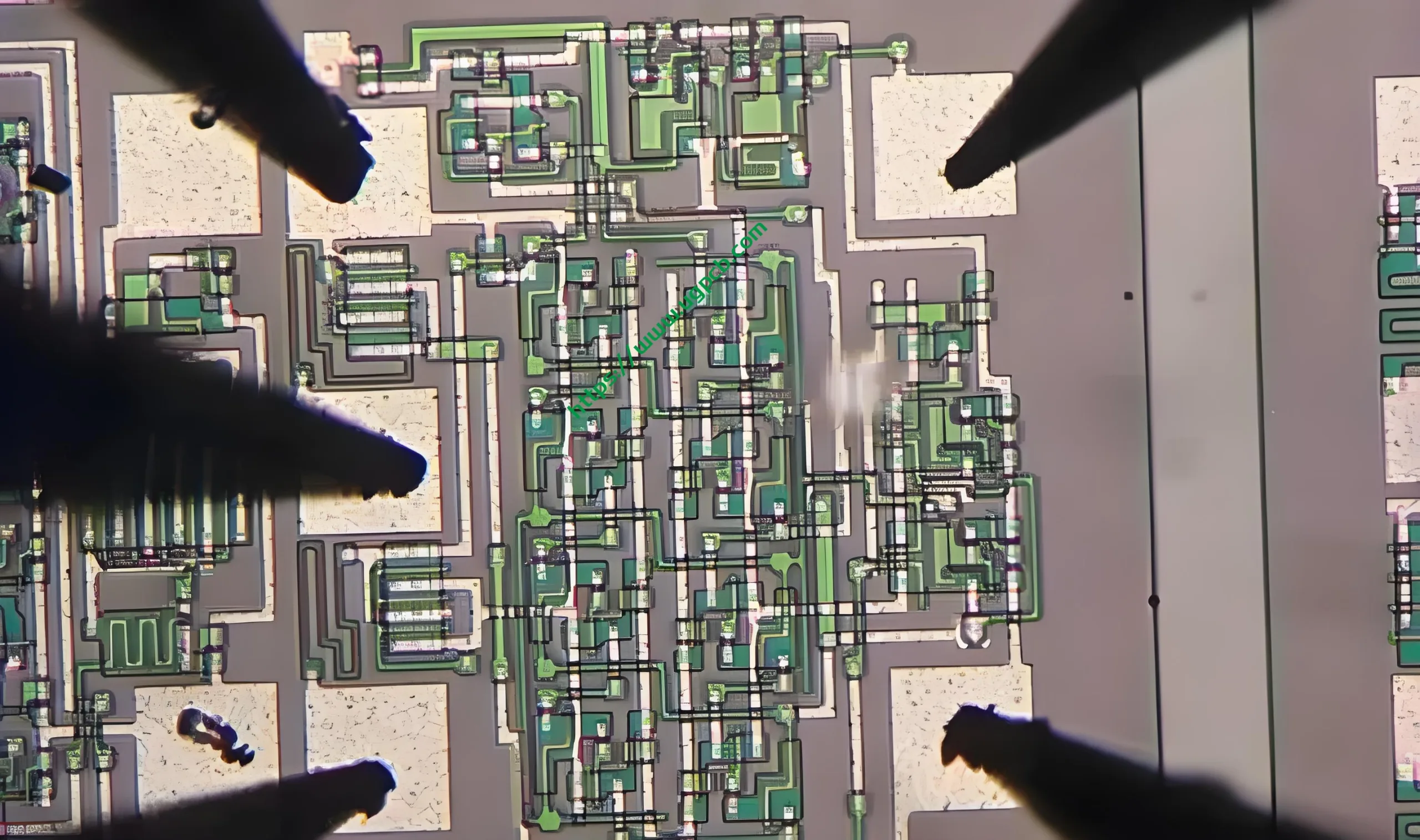
- Modèle de circuit: Les motifs de circuit souhaités sont gravés sur le papier cuivre en utilisant des techniques de gravure de précision.
- Empilement de calques et stratification: Plusieurs couches sont empilées et laminées ensemble, Assurer un alignement et un lien précis.
- Forage et placage: Les trous sont forés pour le montage des composants et l'interconnexion, and then plated to enhance conductivity.
- Application de finition de surface: The immersion gold (5U) coating is applied to provide corrosion resistance and solderability.
- Inspection et test finaux: Le PCB subit une inspection et des tests rigoureux pour garantir la conformité aux spécifications et aux exigences de performance.
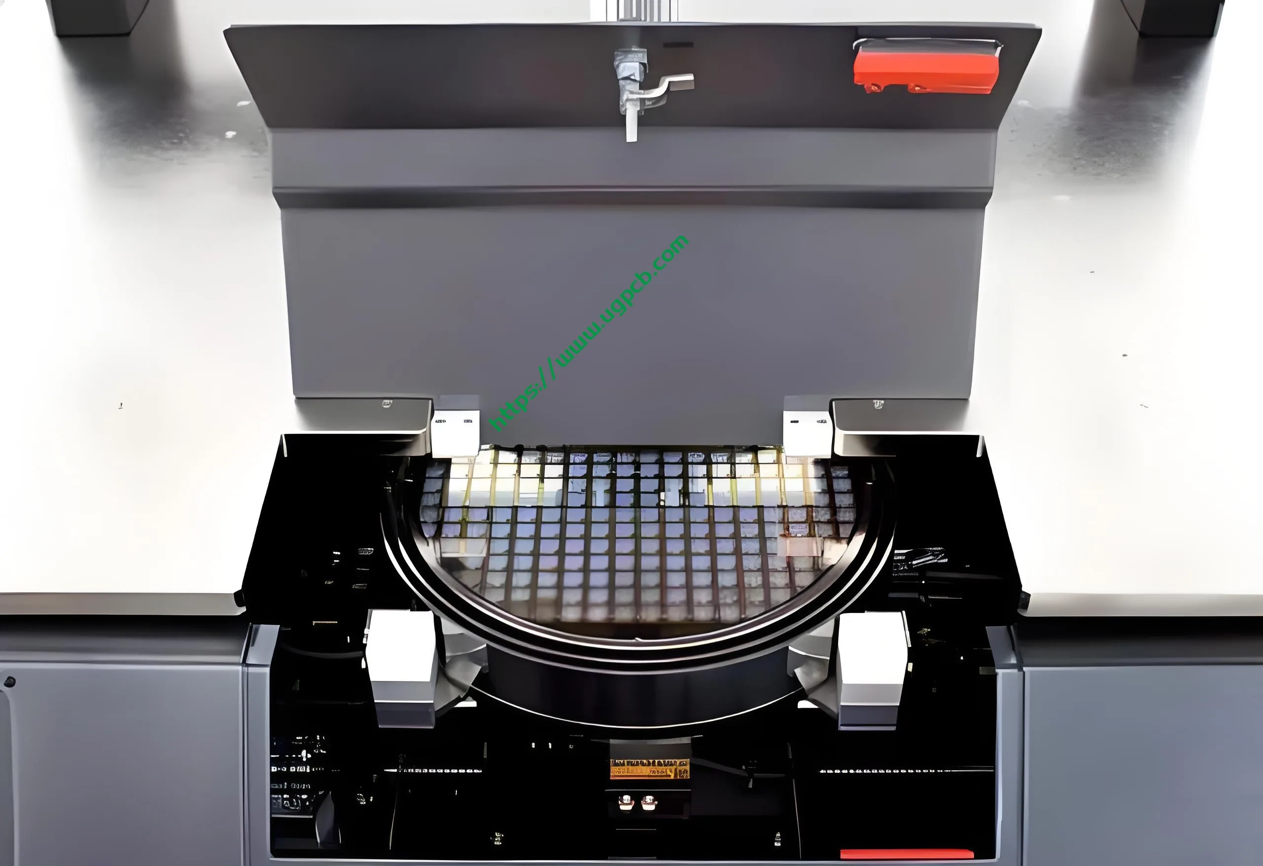
Scénarios d'application
ATE test chip PCBs are primarily used in automated test equipment systems for the testing and validation of semiconductor chips. Ils sont essentiels dans l'industrie des semi-conducteurs, where high-reliability testing is crucial for ensuring the quality and performance of chips before they are integrated into electronic devices. By utilizing ATE test chip PCBs, manufacturers can quickly and accurately identify any defects or issues in the chips, ensuring that only high-quality products are shipped to customers.


