

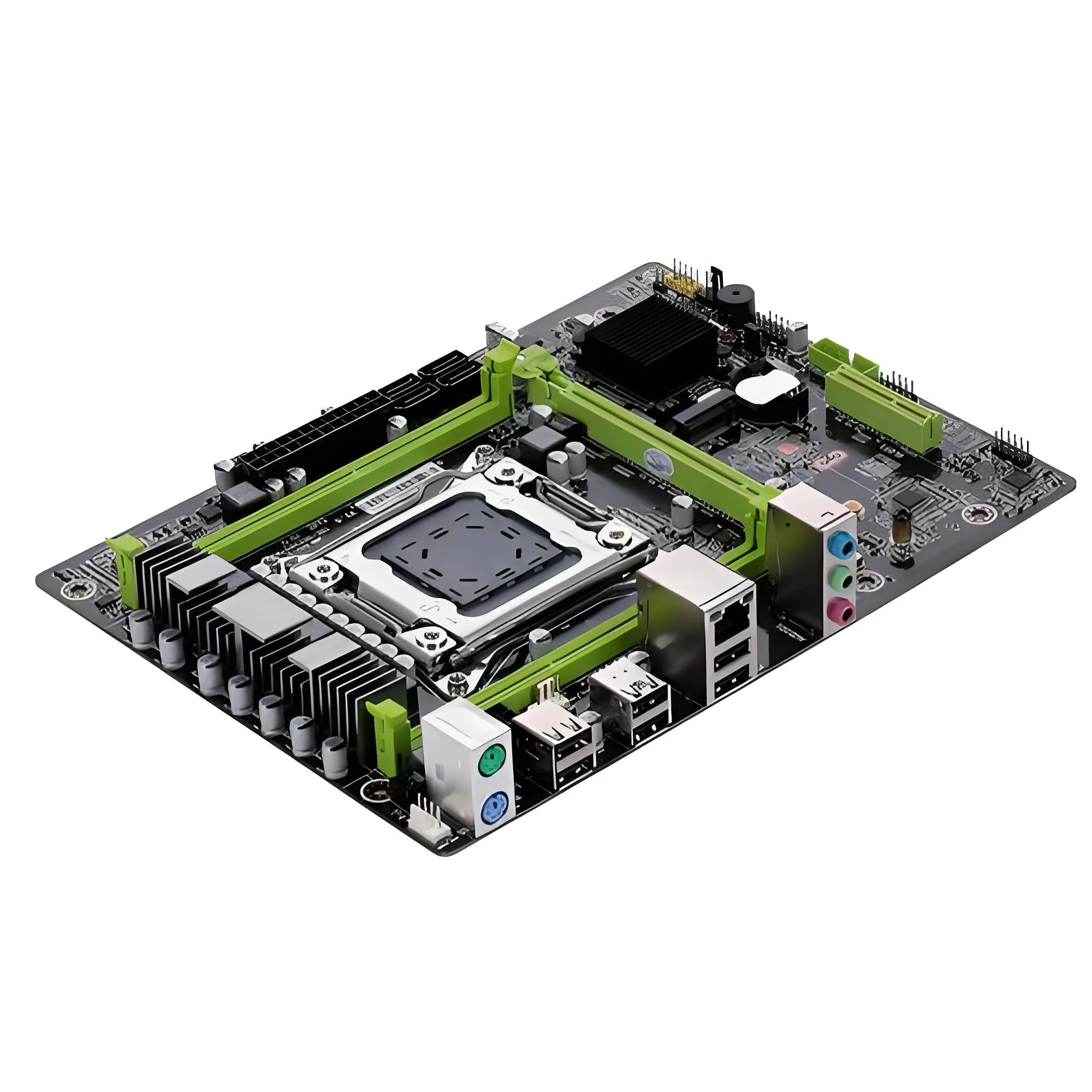
What is a BGA PCB?
A Ball Grid Array (BGA) Circuit imprimé (PCB) is a type of circuit imprimé that features a grid of solder balls on its underside, used for connecting composants électroniques to the board. This design allows for higher input/output connection density and improved electrical performance compared to traditional through-hole or surface-mount technology (CMS) PCB.
Exigences de conception
Designing a BGA PCB involves several key considerations:
- Matériel: Typically made from FR-4, a composite material known for its excellent electrical properties and affordability.
- Nombre de couches: Multilayer designs are common, providing more space for complex circuitry.
- Épaisseur du cuivre: Generally specified as 1/1OZ, balancing conductivity with cost-effectiveness.
- Traitement de surface: Often includes immersion gold to enhance solderability and protect against oxidation.
- Trace and Space: Minimum trace and space are typically set at 4mil, allowing for fine details in the circuit design.
Comment ça marche?
The BGA PCB functions by providing a platform where electronic components can be mounted and interconnected using a grid of solder balls. These balls are aligned in a pattern on the underside of the board, corresponding to contact pads on the component. When heat is applied, the solder melts and creates a strong bond, ensuring reliable electrical connections.
Applications
Due to their high density and reliability, BGA PCBs are widely used in various electronic products including:
- Computer motherboards
- High-performance servers
- Networking equipment
- Advanced consumer electronics like gaming consoles and smart devices
Classification
BGA PCBs can be classified based on several factors:
- Par matériau: Most commonly made from FR-4 due to its balance of cost, force, et propriétés électriques.
- Par nombre de couches: Can range from double-sided to multilayer configurations, en fonction de la complexité du circuit.
- Par traitement de surface: Options include immersion gold, hasl, or organic solderability preservatives (OSP), each offering different levels of protection and solderability.
Matériaux utilisés
La primaire matériels used in manufacturing BGA PCBs include:
- FR-4: A glass-reinforced epoxy laminate that provides excellent mechanical strength and thermal stability.
- Cuivre: Used for the conductive layers, with thickness varying based on design requirements.
- Masque de soudure: Typically green or white, il protège les traces de cuivre de l'oxydation et des courts-circuits accidentels.
- Immersion Or: A surface treatment that improves solderability and protects against corrosion.
Caractéristiques de performance
Key performance attributes of a BGA PCB include:
- Densité élevée: Allows for more components to be packed into a smaller area.
- Fiabilité: The use of solder balls reduces the risk of mechanical failure due to vibration or impact.
- Intégrité du signal: Improved due to shorter signal paths and reduced crosstalk.
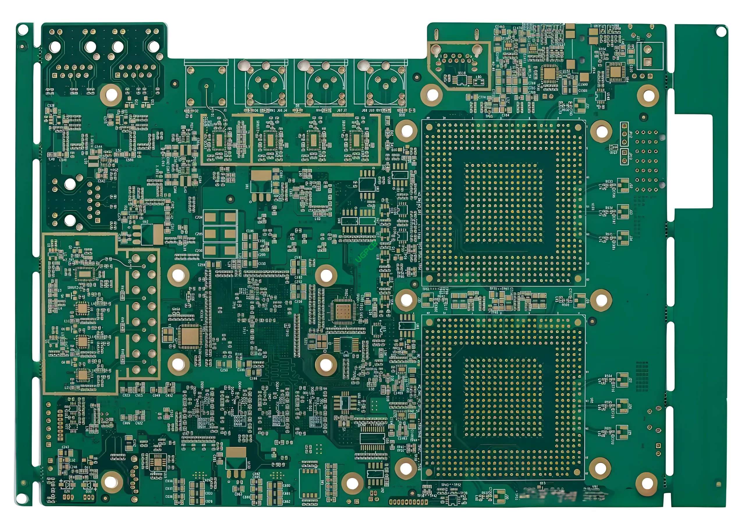
Composition structurelle
Structurellement, a BGA PCB comprises:
- Couches conductrices: Made of copper, etched into the desired circuit patterns.
- Couches isolantes: Éviter les courts-circuits électriques entre les couches conductrices.
- Solder Balls: Arranged in a grid pattern on the underside of the board for component attachment.
Caractéristiques distinctives
Some notable features of a BGA PCB are:
- Fine Pitch: Allows for high-density interconnects, making it ideal for compact devices.
- Robustness: The use of solder balls provides a strong mechanical bond between the board and components.
- Versatilité: Suitable for a wide range of applications due to customizable layer counts and material choices.
Processus de production
The manufacturing process of a BGA PCB involves several steps:
- Conception et disposition: Utiliser un logiciel spécialisé pour créer le modèle de circuit.
- Préparation des matériaux: Découpe des matériaux de base sur mesure et nettoyage des surfaces.
- Laminage: Empiler et coller des couches individuelles sous chaleur et pression.
- Gravure: Enlever l'excès de cuivre pour former les chemins de circuit souhaités.
- Placage: Ajout d'une fine couche de métal aux vias et aux zones de cuivre exposées.
- Application du masque de soudure: Applying the green or white coating to protect traces.
- Traitement de surface: Applying immersion gold or other treatments for solderability.
- Inspection finale: Assurer la qualité et la fonctionnalité avant expédition.
Cas d'utilisation
Common scenarios where a BGA PCB might be employed include:
- Applications d'interconnexion haute densité dans les appareils mobiles.
- Systèmes de communication avancés nécessitant une faible perte de signal.
- Instruments médicaux portables nécessitant des performances fiables dans des environnements difficiles.
- L’électronique automobile exigeant robustesse et longévité.
En résumé, the BGA PCB represents a significant advancement in printed circuit board technology, offrant une complexité et des performances inégalées pour les applications électroniques modernes. Sa flexibilité de conception, combiné à une intégrité et une durabilité supérieures du signal, makes it an essential component in the development of next-generation electronic products and beyond


