

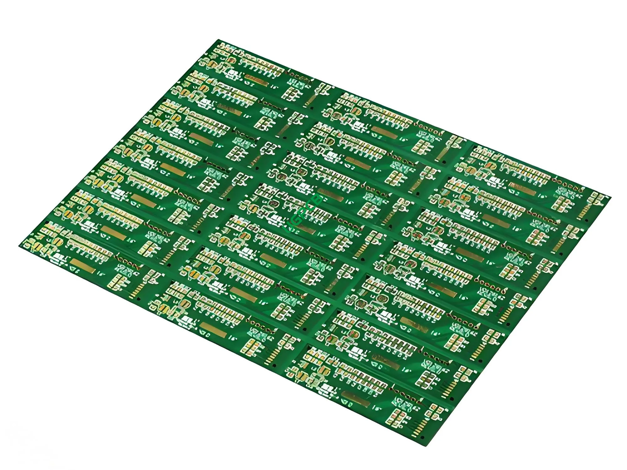
Overview of the P2.9 LED Printed Circuit Board
The P2.9 LED Printed Circuit Board (PCB) is a specialized PCB designed for use with P2.9 LED modules, which are commonly used in high-resolution display applications. This PCB is ideal for creating large, seamless LED displays.
What is a P2.9 LED Printed Circuit Board?
A P2.9 LED Printed Circuit Board is a circuit imprimé (PCB) specifically designed to accommodate and connect P2.9 LED modules. Le terme “P2.9” refers to the pixel pitch of the LED module, which measures 2.9 millimeters between each pixel. This PCB ensures that the LED modules can be interconnected efficiently, providing a stable platform for the electronic components.
Exigences de conception
The design requirements for a P2.9 LED Printed Circuit Board are stringent to ensure its performance and reliability:
- Matériel: SY1000-2 TG170 FR4, choisi pour ses excellentes propriétés électriques et thermiques.
- Nombre de couches: 6 layers to accommodate the necessary circuitry and signal integrity.
- Couleur: Black/White for easy identification and aesthetic appeal.
- Épaisseur finie: 1.0mm pour fournir une intégrité structurelle et une durabilité.
- Épaisseur du cuivre: 1Oz pour assurer une conductivité et une dissipation de chaleur adéquates.
- Traitement de surface: Immersion de l'or pour améliorer la soudabilité et la résistance à la corrosion.
- Minimum Trace and Space: 4mil(0.1mm) to support fine circuit patterns.
- Caractéristiques: More pads with small spacing to accommodate the dense layout of P2.9 LED modules.
Comment ça marche?
The P2.9 LED Printed Circuit Board works by providing a platform for various electronic components to be interconnected through conductive pathways. Ces voies, ou traces, sont en cuivre et sont gravés sur la planche. The SY1000-2 TG170 FR4 material ensures that the PCB can withstand the demands of LED display applications, while the immersion gold surface treatment ensures that these traces remain conductive and resistant to corrosion.
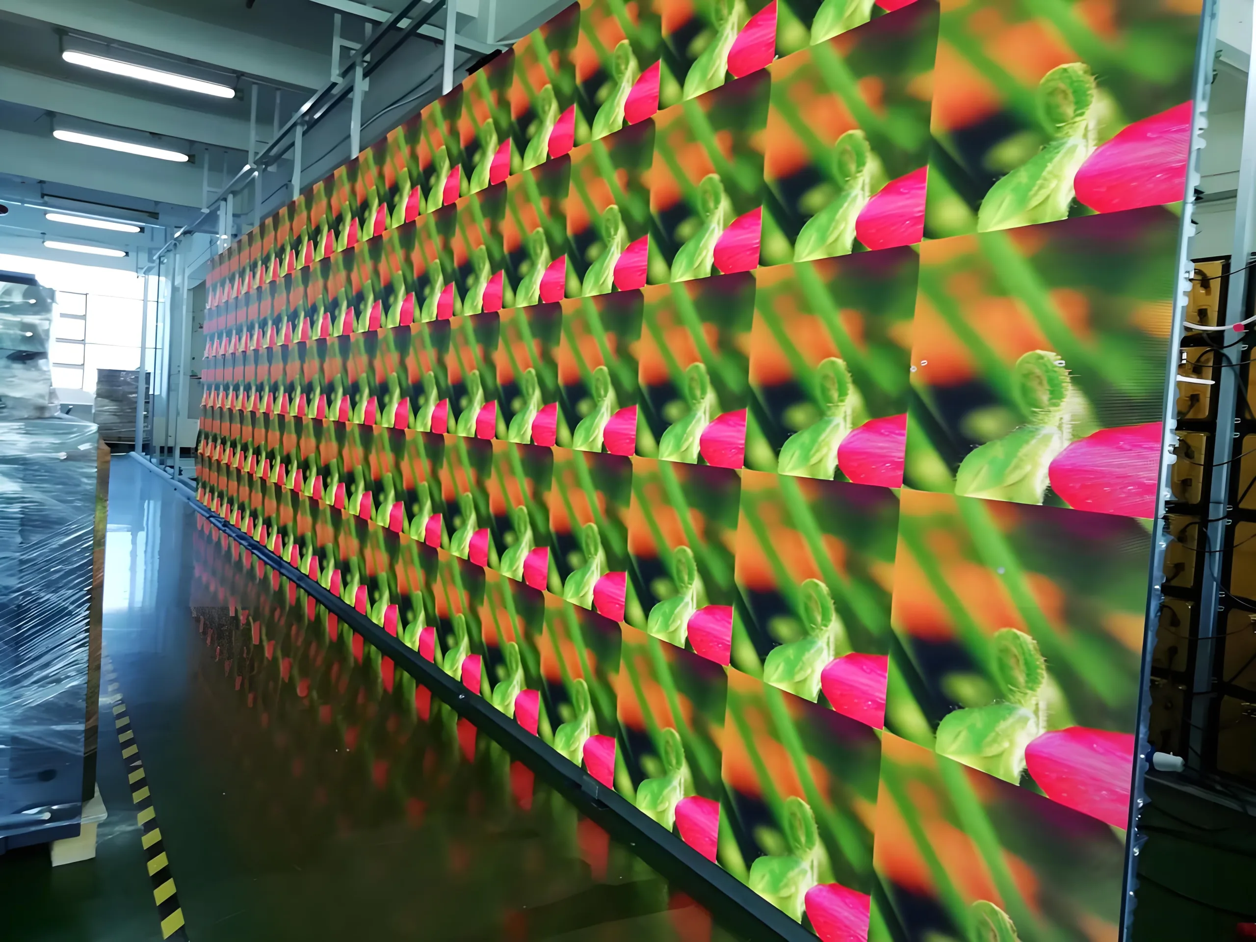
Applications
The primary application of the P2.9 LED Printed Circuit Board is in high-resolution LED display systems where it manages and regulates the flow of electrical signals. Cela comprend:
- Indoor and outdoor LED displays
- Digital signage
- Large format video walls
- Event stages and concert screens
Classification
En fonction de ses fonctionnalités et applications, the P2.9 LED Printed Circuit Board can be classified as a high-density, high-speed digital PCB designed for LED display applications. This classification highlights its capability to handle high-frequency signals and provide stable electrical connections.
Composition des matériaux
Le noyau matériel used in the P2.9 LED Printed Circuit Board is SY1000-2 TG170 FR4, a high-performance composite material known for its excellent mechanical, thermique, et propriétés électriques. This material ensures that the PCB can withstand the demands of LED display applications.
Caractéristiques de performance
The performance characteristics of the P2.9 LED Printed Circuit Board include:
- High signal integrity
- Low signal loss
- Gestion thermique supérieure
- Résistance mécanique robuste
- Stabilité à long terme
Détails structurels
The structural details of the P2.9 LED Printed Circuit Board are as follows:
- Nombre de couches: 6 couches
- Épaisseur finie: 1.0mm
- Épaisseur du cuivre: 1once
- Traitement de surface: Immersion Or
- Minimum Trace and Space: 4mil(0.1mm)
- Caractéristiques: More pads with small spacing to accommodate the dense layout of P2.9 LED modules.
Caractéristiques et avantages
The key features and benefits of the P2.9 LED Printed Circuit Board include:
- Interconnectivité à haute densité
- Excellente intégrité du signal
- Construction mécanique robuste
- Performance fiable à long terme
- Options de couleurs esthétiques (Noir / blanc)
Processus de production
The production process of the P2.9 LED Printed Circuit Board involves several steps including:
- Sélection des matériaux: Choosing high-quality SY1000-2 TG170 FR4 material.
- Empilement de calques: Arrangeant le 6 couches avec précision.
- Gravure: Supprimer l'excès de cuivre pour former les modèles de trace souhaités.
- Application du masque de soudure: Applying a solder mask layer to protect the copper traces.
- Placage: Appliquer un traitement de surface en or d'immersion.
- Assemblée: Incorporer les PTH et les vias pour les interconnexions de couche.
- Essai: Assurer que le PCB répond à toutes les spécifications de performance.
Cas d'utilisation
The P2.9 LED Printed Circuit Board is used in various scenarios such as:
- High-resolution indoor and outdoor LED displays
- Digital signage installations
- Concert and event stages with large video walls
- Retail environments with dynamic advertising screens


