

EMC (전자기 호환성) 디자인은 PCB 엔지니어들은 군 사령관에게 전장 전술을 중요하게 생각합니다. 한 번의 실수로 전체 캠페인에 비용이 발생할 수 있습니다.. 오늘날의 고속 디지털 시스템과 혼합 RF 회로 시대, ~ 위에 85% 복사 방출 실패의 원인은 필터링의 PCB 수준 결함으로 거슬러 올라갑니다., 불연속 차폐 구조, 또는 잘못된 접지 전략. EMC 문제는 결코 고립된 결함이 아닙니다.; 그것은 시스템의 붕괴다.
EMC 설계는 궁극적으로 3차원에서 작동합니다.: 차폐, 필터링, 그리고 접지 – 차폐는 케이지 내부의 간섭을 트랩합니다., 필터링은 라인의 간섭을 차단합니다., 접지는 간섭을 피할 수 있는 경로를 제공합니다.. 이 세 가지 요소가 성의 방어 시스템을 구성합니다.: 쉴드는 벽이다, 필터링이 관문이다, 접지는 해자입니다. 두꺼운 벽은 문이 열려 있으면 쓸모가 없습니다; 튼튼한 문은 해자가 없으면 쓸모가 없다.
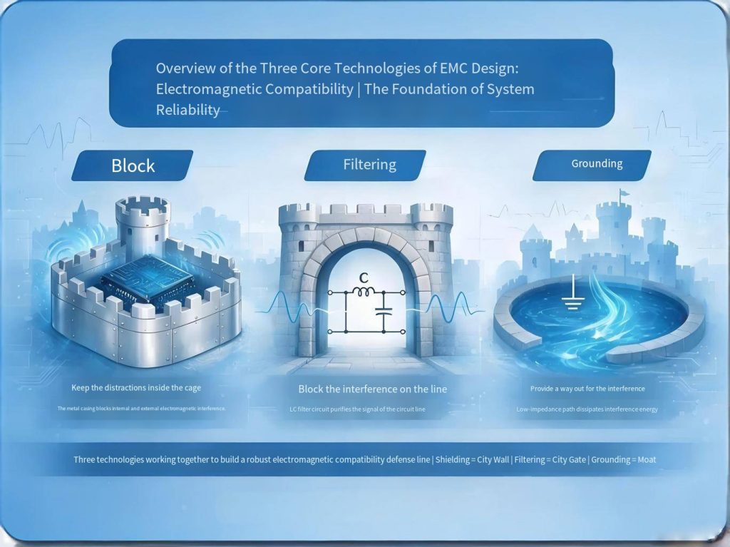
장 1: 차폐 – 케이지에 간섭을 가두기
1.1 쉴드의 본질
차폐는 전도성 또는 자성 재료를 사용하여 밀폐된 표면을 형성합니다.. 이 표면은 정의된 영역 내에서 전자기장을 제한하거나 외부 필드가 유입되는 것을 방지합니다.. 차폐 주소공간적 결합 – 즉 용량성 결합, 유도 결합, 및 복사 결합.
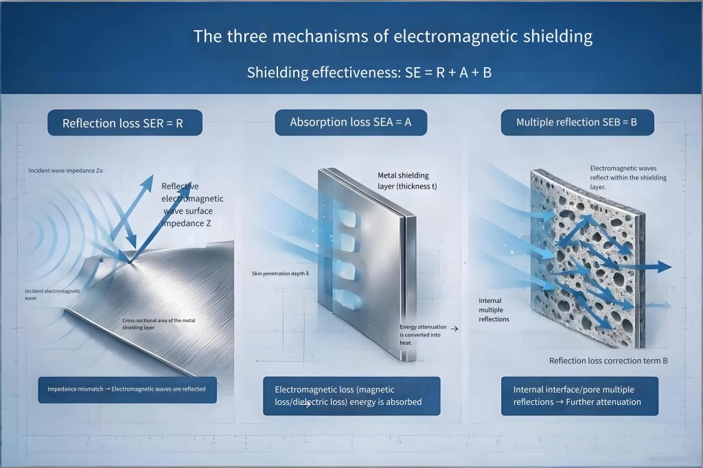
전자파가 차폐물을 만났을 때, 세 가지 현상이 일어난다:
| 기구 | 원칙 | 주요 영향 요인 |
|---|---|---|
| 반사 손실 (아르 자형) | 임피던스 불일치로 인한 차폐 표면의 파동 반사 | 재료 전도성, 파동 임피던스 불일치 |
| 흡수 손실 (에이) | 침투하는 동안 열로 변환된 파동 에너지 | 재료 전도성, 침투성, 두께 |
| 다중 반사 (비) | 쉴드 내에서 반복되는 내부 반사 | 쉴드 두께, 내부 구조 |
총 차폐 효과: SE = R + 에이 + 비 (DB)
흡수 손실 A는 다음과 같이 계산할 수 있습니다.A = 8.69 × (t/d), 여기서 t는 차폐 두께이고 δ는 피부 깊이입니다.. 이는 다음을 의미합니다.차폐 재료의 하나의 피부 깊이는 대략 9 dB의 흡수 손실; 두께를 두 배로 늘리면 또 다른 두께가 추가됩니다. 9 DB.
1.2 전기장 차폐 대. 자기장 차폐
| 비교 | 전기장 차폐 | 자기장 차폐 |
|---|---|---|
| 간섭원 | 고전압, 낮은 전류 | 고전류, 저전압 |
| 재료 선택 | 높은 전도성 (구리, 알류미늄) | 높은 투과성 (철, 뮤메탈) |
| 원칙 | 전기장을 반영, 반대 필드를 생성 | 채널 자속, 그 안에 집중시킨다 |
| 접지 요구 사항 | 접지되어야 합니다. | 필수는 아님 |
| 두께 요구 사항 | 얇으면 충분 (피부 효과) | 충분한 두께가 필요합니다 |
1.3 5가지 중요한 차폐 설계 규칙
- 재료 선택: 전기장 및 원거리장에는 구리 또는 알루미늄을 사용합니다.; 저주파 자기장에는 강자성 재료를 사용합니다..
- 솔기 제어: 솔기 길이를 λ/20 미만으로 유지하세요; 전도성 개스킷을 사용하세요.
- 조리개 제어: 구멍 치수를 λ/20 미만으로 유지하십시오.; 개구부 수를 최소화.
- 케이블 관통: 관통 지점에는 필터링된 커넥터 또는 차폐 어댑터를 사용하십시오..
- 접지: 실드는 잘 접지되어야 합니다.; 그렇지 않으면, 안테나가 된다.
차폐에는 한계가 있습니다.. 저주파 자기장은 차폐하기가 매우 어렵습니다. (두꺼운 강자성 물질이 필요한). 구멍과 솔기로 인해 성능이 심각하게 저하됩니다.. 차폐 비용이 비싸다, 무거운, 그리고 제조가 복잡합니다.차폐는 최후의 방어선입니다. 소스 제어 및 필터링을 먼저 우선시합니다..
장 2: 필터링 – 회선 간섭 차단
2.1 필터링의 본질
필터링은 신호 경로에 주파수 선택 네트워크를 삽입합니다.. 이 네트워크는 간섭을 차단하면서 원하는 신호를 전달합니다.. 주소 필터링전도성 커플링 – 케이블을 통해 전파되는 간섭.
저역 통과 필터 대부분의 간섭은 고주파수이고 유용한 전력 및 신호는 저주파이기 때문에 EMC 애플리케이션에서 가장 일반적인 유형입니다..
2.2 전력 EMI 필터 - 클래식 EMC 필터
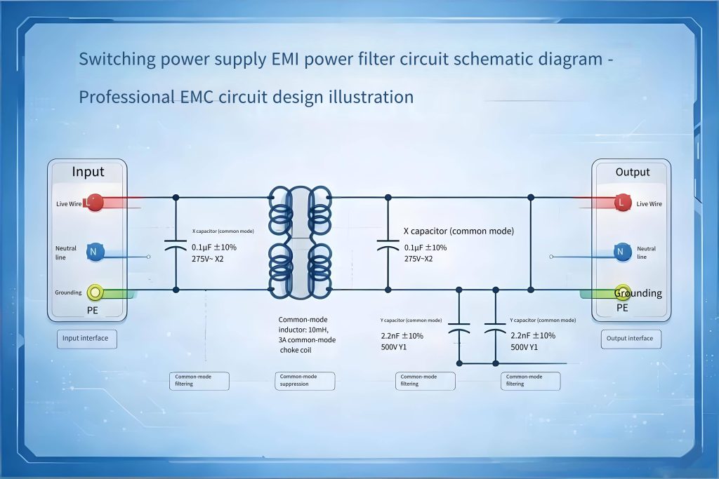
전력 EMI 필터는 스위치 모드 전원 공급 장치의 표준 장비입니다.. 일반적인 구조는 X 커패시터로 구성됩니다., Y 커패시터, 라이브 사이에 연결된 공통 모드 초크, 중립적, 및 접지선.
| 요소 | 억제 모드 | 일반적인 매개변수 |
|---|---|---|
| X 커패시터 | 차동 모드 간섭 | 0.1-2.2μF |
| Y 커패시터 | 공통 모드 간섭 | 1-4.7nF |
| 공통 모드 초크 | 공통 모드 간섭 | 1-10mH |
| 차동 모드 인덕터 | 차동 모드 간섭 | 수십~수백μH |
2.3 핵심 지표: 삽입 손실
삽입 손실 (일) 필터 성능을 평가하는 핵심 매개변수입니다.. 필터 삽입 전과 후의 부하측 전압의 비율로 정의됩니다.:
IL = 20log₁₀(V₁/V₂) (DB)
당CISPR 17:2011, 수동 EMC 필터링 장치의 무선 간섭 억제 특성을 측정하는 방법을 지정합니다., 고품질 DC 전력 필터는 다음을 달성해야 합니다.공통 모드 삽입 손실 ≥ 40 dB 및 차동 모드 삽입 손실 ≥ 30 DB 건너편에 150 kHz – 30 MHz 전도 방출 대역. CISPR 17 50Ω/50Ω 대칭을 포함한 테스트 구성을 정의합니다. (차동 모드) 그리고 비대칭 (공통 모드) 측정, 0.1Ω/100Ω 및 100Ω/0.1Ω 토폴로지와 같은 50Ω이 아닌 시스템뿐만 아니라.
2.4 4가지 필터 설계 원칙
- 공통 모드 우선, 그런 다음 차동 모드: 공통 모드 간섭은 일반적으로 처리하기가 더 어렵습니다.; 공통 모드 필터 설계 우선순위 지정.
- 소스에 가까운 곳에 두세요: 간섭 소스 또는 민감한 포트에 최대한 가까운 필터를 찾으십시오..
- 마인드 임피던스 매칭: 필터는 소스 임피던스와 부하 임피던스 사이에서 작동합니다.; 임피던스 불일치로 인해 성능이 심각하게 저하됩니다.. CISPR에 따라 17, 비대칭 임피던스 테스트 (예를 들어, 0.1Ω/100Ω) 최악의 조건에서 필터 성능을 검증하는 데 사용해야 합니다..
- 접지 우물: Y 커패시터와 필터의 공통 단자는 낮은 임피던스로 접지에 연결되어야 합니다..
장 3: 접지 – 방해를 피할 수 있는 경로 제공
3.1 접지의 본질
접지는 두 가지 핵심 목적을 제공합니다.: 안전 접지 (결함 전류 경로를 제공하여 인력 보호) 그리고신호 접지 (회로에 대한 기준 전위와 간섭 전류에 대한 낮은 임피던스 복귀 경로 제공). EMC는 주로 신호 접지에 중점을 두고 있습니다..
접지는 다음을 해결합니다.고리 문제 – 간섭 전류에는 낮은 임피던스 복귀 경로가 필요합니다. 부적절한 접지로 인해 의도하지 않은 경로를 통한 간섭 전류 발생, 커플링 생성.
3.2 접지 임피던스 - 인덕턴스는 고주파수에서 지배적입니다.
PCB 트레이스 또는 와이어의 임피던스에는 저항 R과 유도 리액턴스 XL이 포함됩니다.:
Z = R + jXL = R + j2πfL
PCB 추적을 고려하십시오. 10 cm 길이, 1.5 폭이 mm, 그리고 50 μm 두께:
- 저항: R = ρL/s = 0.02 × 0.1 / (1.5 × 0.05) ≈ 0.026 오
- 인덕턴스: 약0.08 μH (0.8 μH/m 자체 인덕턴스)
- ~에 1 MHz, 유도성 리액턴스: XL = 2π × 1×10⁶ × 0.08×10⁻⁶ ≒ 0.5 오 -19 저항의 배!
주요 결론: 고주파에서, 인덕턴스가 임피던스를 지배합니다.접지 경로를 줄이는 것이 임피던스를 줄이는 가장 효과적인 방법입니다.. 견고한 접지면은 가장 낮은 임피던스를 제공합니다.. 평면 도체 (구리박) 원형 도체보다 고주파수 임피던스가 낮습니다. (철사).
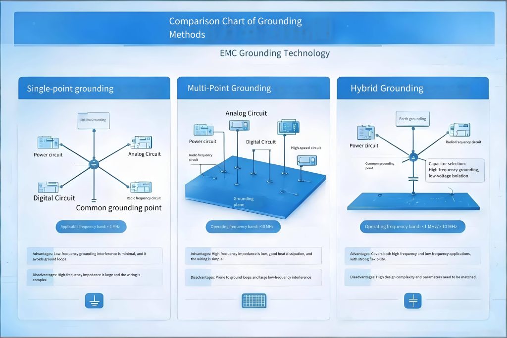
3.3 세 가지 접지 방법
| 접지방법 | 원칙 | 주파수 범위 | 이점 | 불리 |
|---|---|---|---|---|
| 단일점 접지 | 모든 접지 지점은 한 지점에 연결됩니다. | <1 MHz | 접지 루프 없음 | 고주파수에서 높은 임피던스 |
| 다점 접지 | 각 접지점은 접지면에 로컬로 연결됩니다. | >10 MHz | 낮은 고주파 임피던스 | 접지 루프 가능 |
| 하이브리드 접지 | 저주파의 단일 지점, 고주파수의 다중 지점 | 광대역 | 낮은 주파수와 높은 주파수의 균형을 유지합니다. | 복잡한 디자인 |
실제로, 대부분의 제품에는 저주파 회로와 고주파 회로가 모두 포함되어 있습니다.하이브리드 접지는 주류 엔지니어링 접근 방식입니다. – 저주파 구간에 대한 단일점 접지 (접지 루프 방지) 고주파 부분에 대한 다점 접지 및 (임피던스 감소). 커패시터와 인덕터로 가능 “주파수 선택적 접지.”
3.4 견고한 접지면의 장점
견고한 접지면은 전류에 대한 저임피던스 복귀 경로를 제공합니다., 소음을 줄입니다, 회로 신뢰성을 향상시킵니다.. 다층 보드에서, PCB의 넓은 영역을 접지에 할당하고 가능한 가장 짧은 경로를 따라 구성 요소를 연결하여 접지 임피던스를 최소화합니다.. 연속 접지면은 고속 또는 민감한 트레이스 아래에서 차폐 역할을 합니다., 표유 전자기장을 흡수, 누화 감소, EMC 성능을 향상시킵니다..
장 4: 삼자 시너지 – 1+1+1 > 3
4.1 시너지가 필수적인 이유
각 기술 - 차폐, 필터링, 및 접지 - 단독으로 사용할 경우 제한이 있음. 하지만 둘이 같이 일하면, 효과가 배가된다:
| 대본 | 결과 |
|---|---|
| 쉴드가 접지되지 않음 | 거의 쓸모가 없다; 실드는 보조 라디에이터가 됩니다. |
| 필터가 접지되지 않음 | 고주파 필터링 실패 |
| 불량한 접지 시스템 | 방패가 안테나가 된다; 필터가 결합 경로가 됨 |
| 세 사람 모두 함께 일해요 | 최대 효과 |
4.2 사례 연구: 스위치 모드 전원 공급 장치 EMC 설계
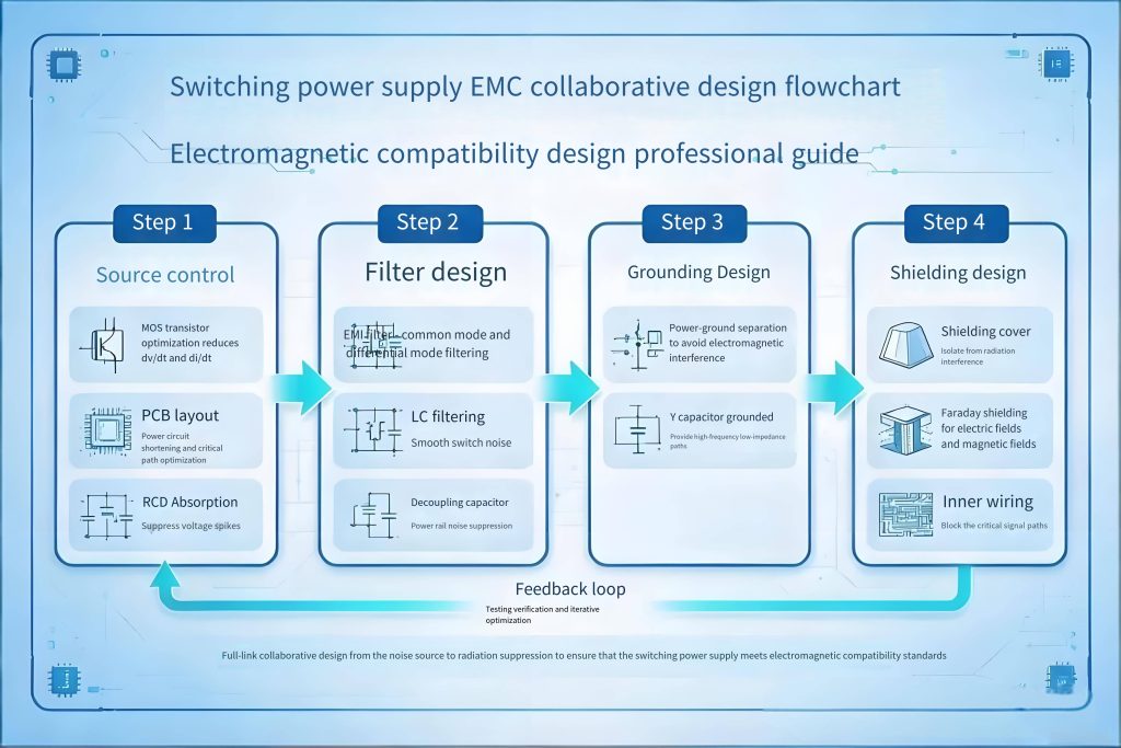
단계 1 – 소스 제어: MOSFET 게이트 드라이브 최적화 (스위칭 슬루율 감소). 최적화 PCB 레이아웃 (전력 루프 영역 최소화). RCD 스너버 회로를 추가합니다.전력 루프 영역을 다음과 같이 줄입니다. 50% 복사 방출을 대략적으로 낮출 수 있습니다. 12 DB.
단계 2 – 필터 설계: X 커패시터 설치, 공통 모드 초크, 입력의 Y 커패시터 (전력 EMI 필터). 출력에 LC 필터 추가. 제어 IC 전원 핀에 디커플링 커패시터 배치.
단계 3 – 접지 설계: 신호 접지와 전원 접지를 분리하세요.; 단일 지점에서 연결. Y 커패시터를 섀시에 로컬로 접지. 방열판 접지.
단계 4 – 차폐 설계: MOSFET 및 정류기 위에 차폐 캔 추가. 변압기에 패러데이 쉴드 레이어 추가. 양쪽에 접지면이 있는 내부 레이어에 중요한 신호를 라우팅합니다..
4.3 사례 연구: 고속 디지털 보드 EMC 설계
단계 1 – 소스 제어: 제어 신호 상승 시간 (직렬 종단 저항기). I/O 커넥터에서 클록 추적을 멀리 유지하십시오.. 차동 쌍을 대칭적으로 라우팅.
단계 2 – 접지 설계: 견고한 접지면 유지; 분열을 피하다. I/O 영역을 위한 별도의 접지면 섹션을 지정하고 이를 섀시에 연결합니다..
단계 3 – 필터 설계: I/O 라인에 공통 모드 초크 추가. 전력 진입점에서 π형 필터 사용. 모든 IC 전원 핀에 디커플링 커패시터를 배치합니다.표준 6층 보드 스택업에서, 레이어의 견고한 접지면 2 그리고 5 전체에 걸쳐 15-25dB의 방사선 억제 기능을 제공합니다. 30 MHz - 1 GHz 대역.
단계 4 – 차폐 설계: 차폐된 I/O 커넥터 사용. 섀시 이음새에 전도성 개스킷 적용. 내부 레이어에 중요한 신호 라우팅.
장 5: 디자인 우선순위 – 소스 제어가 항상 최우선입니다
5.1 5중 방어
| 층 | 측정하다 | 효과 | 비용 |
|---|---|---|---|
| 층 1 | 소스 제어 (구성 요소 선택, 레이아웃 최적화) | 근본적인 해결책 | 가장 낮습니다 |
| 층 2 | 루프 디자인 (루프 영역 최소화, 임피던스 매칭) | 상당한 개선 | 낮은 |
| 층 3 | 필터링 | 효과적인 억제 | 중간 |
| 층 4 | 접지 | 체계적인 개선 | 중간 |
| 층 5 | 차폐 | 최후의 수단 솔루션 | 제일 높은 |
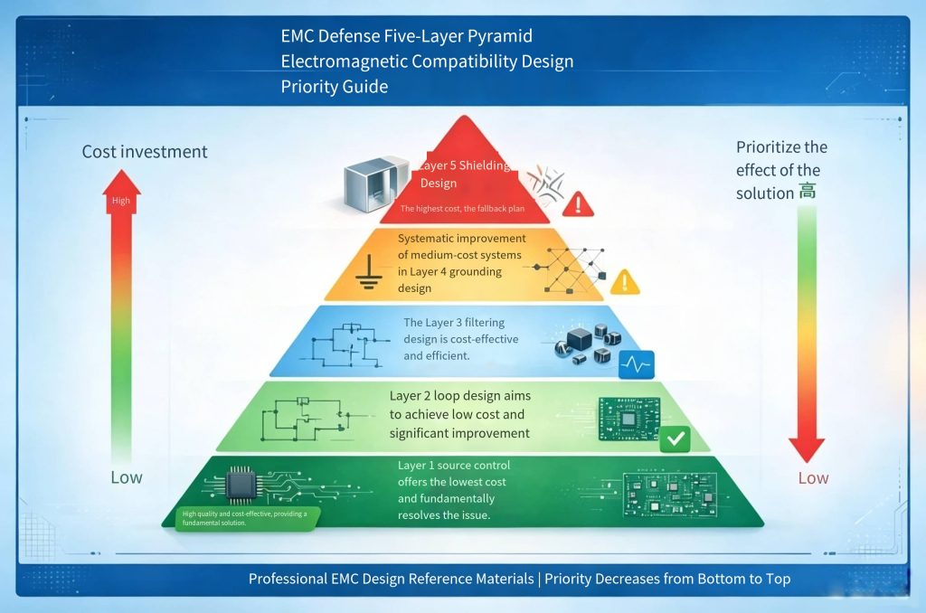
핵심원리: 가능하면 소스에서 해결하세요.; 소스에서 제거할 수 없는 것만 필터링; 방패는 최후의 수단으로만 사용.
5.2 소스 제어가 가장 중요한 이유
| 비교 | 소스 제어 | 교정 조치 (필터링/차폐) |
|---|---|---|
| 효과 | 근본적인 | 증상 치료 |
| 비용 | 거의 0 | 추가 구성요소/재료 필요 |
| 신뢰할 수 있음 | 높은 | 온도/노화로 인해 품질이 저하될 수 있음 |
| 디자인 자유 | 높은 | 공간과 비용의 제약 |
| 생산 일관성 | 좋은 | 부품 공차의 영향을 받음 |
MOSFET 스위칭 속도 감소 30% 고주파 노이즈를 6~10dB까지 낮출 수 있어 어떤 필터보다 효과적입니다..
장 6: EMC 설계 체크리스트 – 빠른 참조
회로도 단계
- □ 전원 입력에는 EMI 필터가 있습니다.; 모든 IC 전원 핀에는 디커플링 커패시터가 있습니다.
- □ 고속 신호에는 종단 저항이 있습니다.
- □ I/O 라인에는 TVS/ESD 보호 기능이 있습니다.
- □ 시계에는 RC 필터링 또는 확산 스펙트럼이 있습니다.
- □ 고전압 섹션과 저전압 섹션 간의 절연은 IPC-2221 요구 사항을 충족합니다.
PCB 레이아웃 단계
- □ 전력 루프 면적 최소화; 서로 가깝게 배치된 전원 장치
- □ 아날로그/디지털/전력/RF 섹션 분할
- □ I/O 커넥터는 함께 그룹화되어 소음원에서 멀리 배치됩니다.
- □ I/O로부터 멀리 떨어진 클럭 트레이스; 양쪽에 접지면이 있는 내부 레이어에 라우팅됨
- □접지면이 견고하게 유지됨; 분열을 피하다
기계/구조 단계
- □ 중요한 소음원에 차폐 캔 추가; 차폐 접지 저항 ≤ 0.1 오
- ❑ 전도성 개스킷으로 처리된 솔기; 간격 길이 < l/20
- ❑ 차폐 케이블 및 커넥터 사용
- □ 방패, PCB 접지, 낮은 임피던스로 연결된 섀시 접지
- □ 통풍구를 λ/20 이하로 유지; 필요한 경우 도파관 통풍구를 사용하십시오
결론: EMC 디자인은 시스템 엔지니어링입니다
EMC 설계는 포인트 솔루션이 아니라시스템 공학.
차폐, 필터링, 접지는 분리할 수 없는 트리오를 형성합니다..
하지만 핵심 원칙을 기억하세요.: 소스 제어가 먼저입니다, 필터링은 미드필더 지원을 제공합니다, 방어는 최후의 방어선이다, 접지는 모든 것을 관통하는 기초입니다..
EMC 연구실의 스펙트럼 분석기에서 춤추는 방출 스파이크에 직면했을 때, 당신이 내린 결정을 다시 추적해 보세요. PCB 설계 도면 – 배치에 대한 모든 선택, 라우팅, 디커플링, 접지, 그리고 차폐 - 이것이 진정으로 성공과 실패를 결정하는 선택입니다..
EMC는 제품으로 측정되지 않습니다.; 그것은 그것에 설계되었습니다.
데이터 소스 설명:
이 기사에 인용된 기술 데이터 및 표준은 다음 출처를 기반으로 합니다.:
- 차폐 효과 공식 SE = R + 에이 + B 및 흡수 손실 공식 A = 8.69 × (t/d) 전자파 차폐 이론 문헌을 참조합니다..
- 삽입 손실 정의 IL = 20log₁₀(V₁/V₂) 그리고 CISPR 17:2011 표준 요구 사항 (공통 모드 ≥40dB, 차동 모드 ≥30dB 150 kHz~30MHz 대역) CISPR에서 참조됩니다. 17:2011 -수동 EMC 필터링 장치의 억제 특성 측정 방법.
- PCB 트레이스 임피던스 계산 R = ρL/s 및 유도성 리액턴스 XL = 2πfL은 PCB 접지 및 간섭 억제 기술 문헌에서 참조됩니다..
- PCB 수준 EMC 데이터 (85% 방사성 방출 실패의 원인이 PCB 수준 문제로 추적됨; 15~25dB의 6레이어 보드 접지면 억제) EMC 문제 해결 및 실제 설계 문헌을 참조합니다..
- PCB 전기 요구 사항에 대한 IPC-2221 표준 프레임워크 (접지, 차폐, 신호 무결성) IPC-2221에서 참조됩니다 –인쇄 기판 설계에 대한 일반 표준.
- UL PCB 안전 표준 (UL 796 견고한 인쇄 배선 기판용) UL에서 참조됩니다. 796 -인쇄 배선 기판 표준.
