
O placă de circuit Mai subțire decât hârtia este acum un câmp de luptă critic în competiția tehnologică globală. De la servere AI la vehicule inteligente, Performanța sa determină în mod direct succesul sau eșecul produselor electronice.
La laboratorul de testare al UGPCB, Inginerii plasează un server AI nou produs PCB într -un mediu cu frig extrem de -55 ° C, apoi transferați-o rapid într-o cameră de temperatură înaltă de 125 ° C după 30 secunde. Acest test dur de ciclu se repetă 1,000 Timpuri-Asigurarea fiecărui circuit la nivel micron menține stabilitatea semnalului în condiții extreme.
“Proiectul nostru aproape a ratat termenul său din cauza interferenței semnalului PCB!” a lamentat o companie tehnologică r&D Director. Cu AI Computing Boom și Smart Vehicle Electronic Architecture Revolution, Fabricarea PCB de înaltă calitate este supusă unei transformări tehnologice fără precedent și concurența capacității.
01 Analiza lanțului industrial: Sistemul circulator de fabricație PCB
PCB -uri, Salut ca “Mama electronică,” Formați scheletul de bază al aproape toate dispozitivele electronice. Ca platformă fundamentală pentru componente, Ei permit conectivitatea electrică critică. Calitatea lor determină direct fiabilitatea produsului final, durată de viaţă, și competitivitatea pieței.
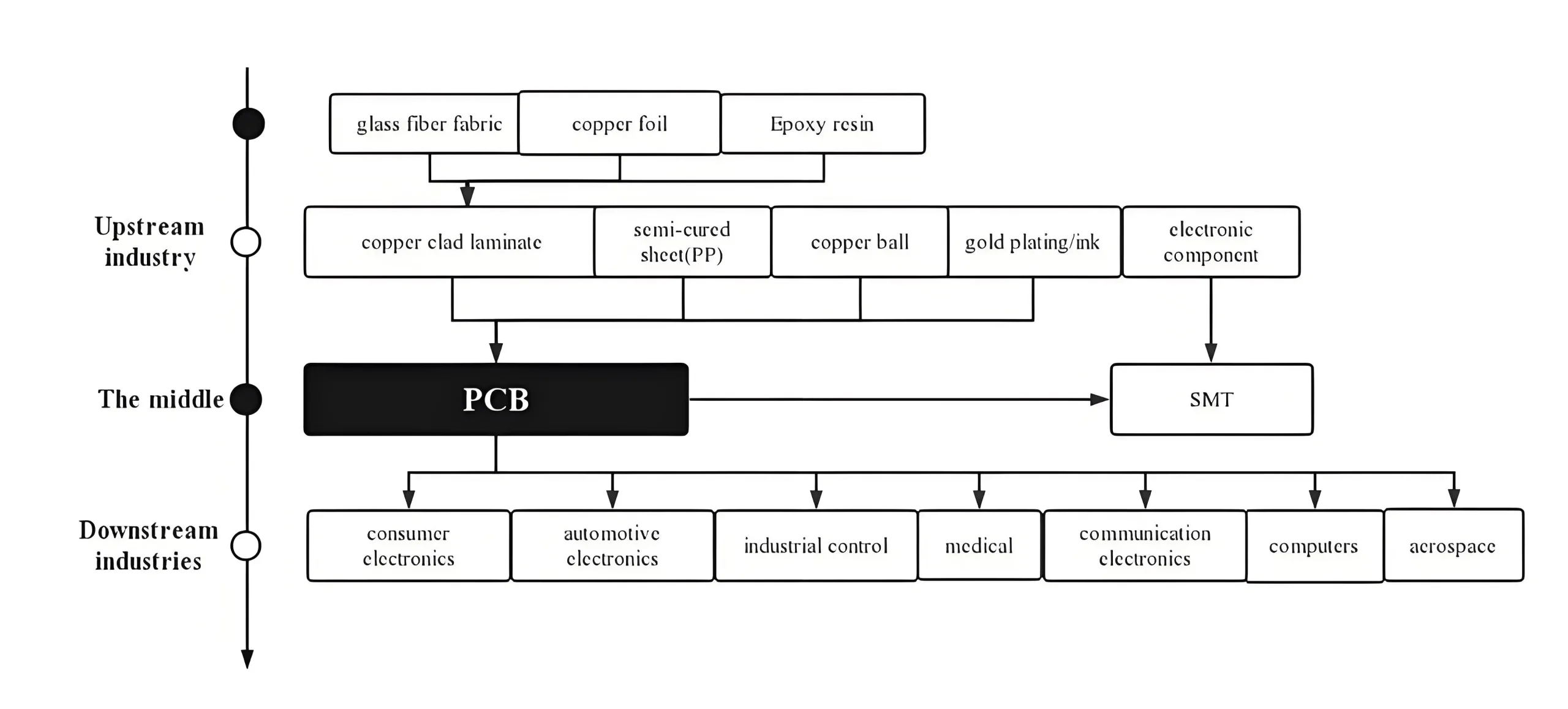
În amonte: The “Trei regate” Luptă în materii prime
Materiile prime constituie 60% de costuri PCB, cu laminat îmbrăcat în cupru (Ccl) singur contabil pentru 27.31%. CCL este un material compozit care cuprinde:
-
Folie de cupru (42.1% Cost CCL): Serverele AI determină cererea crescândă de folie scăzută (puritate ≥99,99%)
-
Țesătură electronică din fibră de sticlă (~ 27% cost): 5G stații de bază & Serverele AI necesită o țesătură de sticlă cu DK scăzută
-
Rășină sintetică: Cererea de rășină pe bază de apă crește 15% Da, condus de ROH -uri UE & Eco-standarde din China
Midstream: Precision Engineering în fabricarea PCB
Fabricarea PCB amestecă artă și inginerie. 8+N+3 Panouri HDI Obțineți 2,5 mil/2,5 mil (≈0.063mm) Lățimea liniei/precizia distanțării, cu precizie de foraj cu laser în ± 25μm.
Descoperiri cheie ale proceselor:
-
Optimizarea stivuirii: Reduce prin captura de semnal prin 30% prin simularea impedanței
-
Microvii eșalonate: Atinge 15:1 raporturi de aspect pentru rutarea de înaltă densitate
-
24-Teste de îmbătrânire în oră: Validează fiabilitatea sub 85 ° C/85% RH Stres
Datele Prismark arată 2023-2028 creştere: 18+ Panouri de strat (9% CAGR), China HDI (6% CAGR, lider global), substraturi IC (7% CAGR), PCB -uri flexibile (4% CAGR).
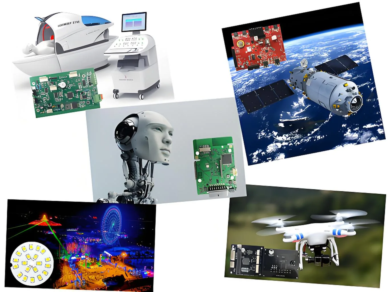
În aval: Creștere explozivă în aplicațiile PCB
Calculul AI și EV -urile inteligente redau cererea PCB:
-
Servere AI: Conduceți volume/prețuri mai mari de PCB; densitate crescută de calcul pe raft + control strict al impedanței pentru Chipsuri AI
-
Vehicule energetice noi (Nevs):
-
Conținut PCB 4-5x Vehicule tradiționale
-
800Platformele V necesită 40% rezistență la tensiune mai mare
-
Senzorii ADAS stimulează cererea de PCB de înaltă frecvență
-
-
Electronică medicală: Dispozitivele implantabile solicită contaminarea ionică ≤1.56μg/cm² (NaCl Eq.), depășind cu mult standardele de consum.
02 Descoperiri tehnologice: Trei bătălii critice în producția avansată de PCB
Revoluția materialului PCB: De la fizică de bază la efecte cuantice
Aplicațiile de înaltă frecvență cer materiale noi. 5G stațiile de bază necesită ± 7% control de impedanță (>10GHz), roman de rășină roman r&D.:
Formula științei materialelor: Df = ε” / e’
(Factor de disipare = pierderi dielectrice / Permisivitate)
Materialele scăzute-DF/DK sunt pivotante. Repere din industrie precum PTFE modificat (Df<0.001) și rășini de hidrocarburi (DF = 0,001-0.002) Reduceți pierderea semnalului mmwave cu peste 60%.
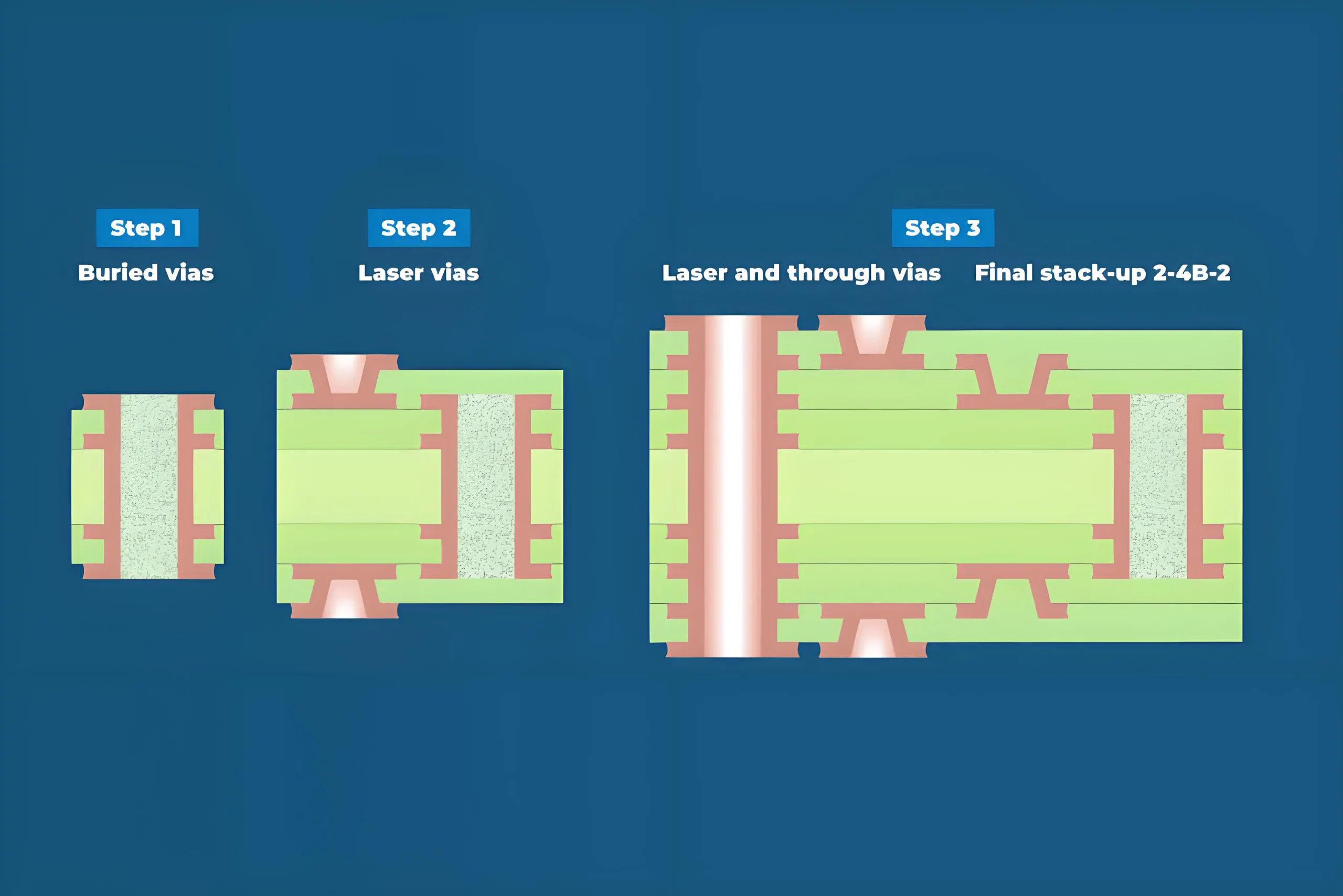
Inovația procesului PCB: Provocări la nivel micron
La fabrica inteligentă a UGPCB, Producerea laserului proces 8-strat 3+N+3 HDI la 300 găuri/secundă. Progrese cheie:
-
Orice strat de interconectare: Permite 15:1 MICROVIAS RATIO DE ASPECT
-
Controlul impedanței: ± 5% toleranță (vs. ± 7% pentru radarul auto)
-
Tehnologie rigidă-flexă: Rezistă >100,000 cicluri de îndoire
Alinierea stratului în 12μm (1/6 păr uman) asigură golul BGA <25% (Clasa IPC-A-610 3), Prevenirea defecțiunilor de lipire a cipurilor.
Evoluția inspecției: De la postproducție la predicție în timp real
Inspecția automată a razelor X îmbunătățite (Axi) stimulează viteza de inspecție BGA 5x, reducerea ratărilor la <0.1%. Analiza avansată a eșecului:
-
Inspecție vizuală (100X microscop)
-
Testare electrică (Analizator de rețea)
-
Radiografie/secțiune transversală (Sem/eds)
-
Imagistica termică (Detectarea spotului fierbinte)
PCB -urile de calitate auto necesită -40 ° C ~ 125 ° C Ciclism termic (1,000 cicluri) cu <0.01% Impedance Drift pentru aplicațiile BMS.
03 Concurență globală: Schimbări de capacitate & Poziționarea tehnologiei
Dinamica regională: Dominanța Asia-Pacific
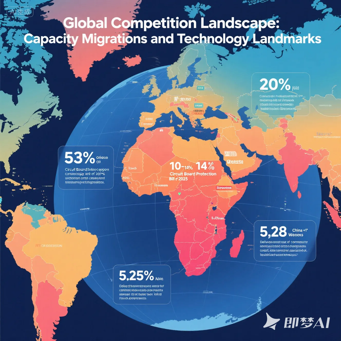
2025 Peisaj PCB: “Condus de est, Creștere multi-polară”:
-
China: 53% Capacitate globală (Prismark)
-
Asia de Sud -Est: 20% Creștere yoy (Tailanda, Vietnam)
-
STATELE UNITE ALE AMERICII: Subvenții prin “Legea privind protecția plăcii de circuit 2025”
Ascensiunea PCB de înaltă calitate din China
În timp ce China conduce în volum, Ieșirea sa rămâne la mijlocul până la mic (81% Plăci rigide). Firmele de frunte sparg barierele:
-
Circuite Shennan: Substraturi FCBGA pentru GPU -uri NVIDIA
-
UGPCB: PCB-uri cu radar MMWave certificat auto
-
Kinwong Electronics: PCB -uri de comunicare prin satelit spacex
Cercetare Nester proiectează piața globală a PCB -ului care ajunge la 155,38 USD de către 2037, cu cota de ultimă generație a Chinei care ar putea crește de la 15% la 35%.
04 Viitoarele câmpuri de luptă: AI & Creșterea unității de electrificare
AI Computing: The “Salt dimensional” pentru PCB -uri
Investiția AI Infrastructure Remodelează tehnologia PCB:
-
Plăci de server AI: >20 straturile acum cuprind 60%
-
Substraturi HBM: Lățimea liniei <8μm
-
Modul optic PCB -uri: 80% Adoptarea materialelor cu pierderi scăzute
AI Server PCB Market CAGR: 16% (Îngheţ & Sullivan). Utilizează telefoanele AI 30% Mai multe straturi și 15 FPCS/Unitate, accelerarea adoptării HDI.
EV Revoluție: Reinginerea automobilului “Inima”
NEV Electronics creează noi standarde PCB auto:
-
Controlere de domeniu: 8-12 strat HDI dominanță
-
Panouri Lidar: Materiale PTFE de înaltă frecvență
-
800V platforme: Izolația rezistă ≥3kV
2025 Vânzări NEV: ~ 15m unități. Valoare PCB/vehicul 4x mașini de gheață. PCB -urile BMS necesită 0.01% Stabilitatea impedanței (-40° C ~ 125 ° C.).
Fabricare durabilă: Imperativul de conformitate
Reglementările EPR ale UE Mandat:
-
100% Lipire fără plumb de 2026
-
95% Rata de reciclare a cuprului
-
≥30% rășini pe bază de bio
Cererea standardelor de emisii din China 40% Reducerea COV, apăsând adoptarea cernelii pe bază de apă în imprimarea PCB din 35% la 65% de 2027.
05 Concluzie: Poziționare strategică & Alegeri
Industria globală a PCB este supusă unei transformări profunde. Mordor Intelligence prognozează creșterea pieței de la 84,24 USD (2025) până la 106,85 USD (2030) la 4.87% CAGR. Oportunități cheie:
-
Capacitate de înaltă calitate: 18+ Panouri de strat (9% CAGR), Lipsa de substrat IC (30%)
-
Schimbare regională: 25% Costuri de configurare mai mici în Asia de Sud -Est
-
Inovație materială: Materiale reduse DK/DF (40% Creșterea cererii)
Nota: Datele prezentate în acest document provin din cele mai recente rapoarte ale instituțiilor autoritare, inclusiv Prismark, IPC, și îngheț & Sullivan. Toți parametrii tehnici au fost validați prin teste riguroase efectuate în laboratoarele acreditate CNAS. Standardele de proces aderă cu strictețe la specificațiile curente ale ediției, cum ar fi IPC-6012EM* și IPC-2221B.
