
Introducere: The Foundation in the Storm’s Eye
Beneath the spotlight on the semiconductor industry, cel Placă de circuit tipărită (PCB) has long played the role of a silent, foundational pillar. Cu toate acestea, in 2025, a raw material price storm, led by gold and copper-clad laminates (Ccl), has thrust PCBs to the forefront of supply chain cost pressures. This storm is no accident; it is the intense collision between exponential demand growth from AI infrastructure expansion and limited supply capacity. This article provides a professional analysis of the PCB industry’s cost challenges and underlying drivers, revealing how profound technological transformation is enabling a leap in value amidst the crisis. It offers critical insights for companies seeking reliable Furnizori de PCB and high-quality PCB services.
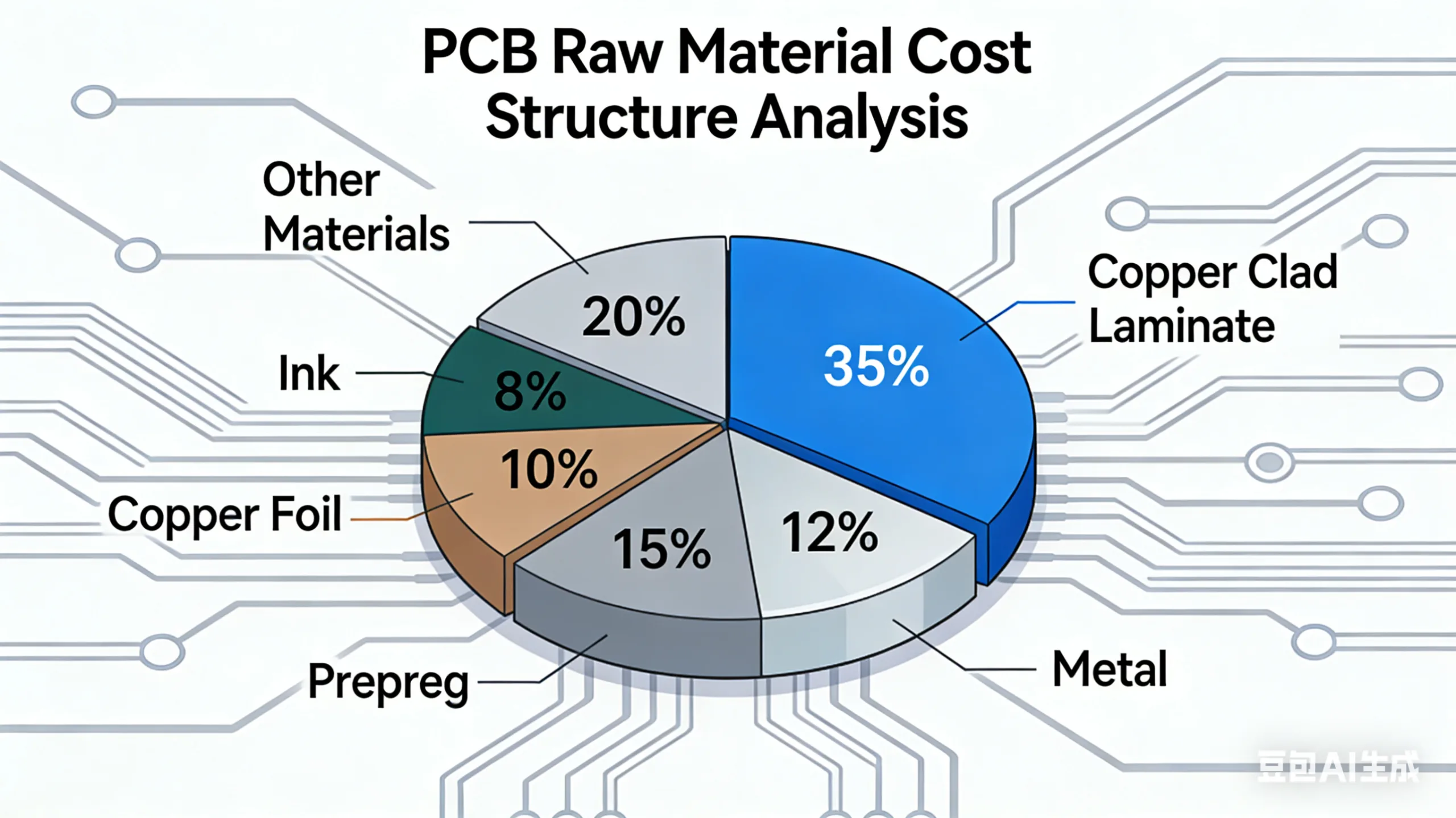
I. Cost Deconstruction: The “Gold and Silver” Straws Breaking the Camel’s Back
The raw material cost structure of a PCB is complex, but gold and copper-clad laminates are undoubtedly the two heaviest “weighted stocks.” According to analysis from the authoritative industry firm Prismark, in a typical multilayer PCB for servers, CCL can account for 30%-40% of the cost, while precious metals like gold used in plating and surface finishes (De ex., De acord) can account for 8%-15%. Together, they approach half of the total material cost. This can be simplified as:
PCB Raw Material Cost ≈ (CCL Cost × Share) + (Precious Metal Cost × Share) + (Other Material Costs)
(Sursă: Prismark Q3 2025 PCB Material Cost Analysis Report)
1. Aur: More Than a Shiny Finish
Gold in high-end PCB -uri is primarily used for surface finishes on critical connections to ensure superior conductivity, oxidation resistance, and solderability. The price of potassium gold cyanide (gold salts), for example, has become an industry barometer. Data from a major Korean Producător de PCB reveals a staggering trajectory: from approximately 50,000 KRW/gram in 2023 la 99,000 KRW/gram in Q3 2025—a near 100% increase. This directly raises the manufacturing cost for PCB-uri HDI and IC substrates using processes like ENIG (Electroless Nickel Immersion Gold). For clients requiring high-volume Ansamblu PCBA, this cost transfer is significant.
2. Copper-Clad Laminates: The Direct Conduit of AI Demand
As the core dielectric carrying circuit patterns, the performance of CCL directly determines the final PCB’s signal integrity, Managementul termic, and reliability. Servere AI, high-speed switches, şi AI accelerator cards impose near-demanding requirements for data throughput and signal loss, driving explosive demand for high-speed/high-frequency, ultra-low loss (De ex., Ultra Low Loss, Very Low Loss grades) laminates.
Feedback from top-tier manufacturers like Samsung Electro-Mechanics—reporting a 10%-15% year-over-year procurement cost increase in Q3—epitomizes this structural supply tension. This is especially true for high-performance laminates used in AI server motherboards şi GPU accelerator card PCBs.
Ii. Deep-Seated Drivers: The AI Frenzy Reshaping the PCB Demand Map
Rising raw material costs are the surface symptom; the core engine is global digital and intelligent transformation, specifically the arms race in AI computing infrastructure.
1. Role Evolution: Din “Connector” la “System-Critical Component”
Tradiţional, PCB -uri were viewed as mechanical supports and electrical connection platforms for components. In the AI era, this role has fundamentally changed. Next-generation architectures, exemplified by platforms like NVIDIA’s Rubin, pursue extremely high internal interconnect bandwidth and density, making high-layer-count PCB -uri (typically 22+ straturi) şi any-layer HDI technology standard. Every trace on the PCB affects data latency and power consumption; its design and manufacturing precision directly impact the synergistic efficiency between CPUs/GPUs, memorie, and accelerators. Industry analysis indicates that an AI server motherboard’s value is multiples that of a standard server, with its PCB portion seeing corresponding increases in technical content and price.
2. Exponential Rise in Demand Specifications
AI training and inference generate specific and stringent PCB requirements:
-
Increased Layer Count: To accommodate more complex power delivery networks and more signal layers, AI server motherboard layer counts are moving toward 30 layers and beyond.
-
Material Upgrades: Data rates moving from 224Gbps and beyond are driving demand for M6, M7 grade ultra-low loss laminates (Df as low as 0.0015).
-
Dimensiune & Integrare: Larger board sizes to integrate more compute units, and advanced processes like embedded component PCB -uri to enhance integration and performance.
According to the IPC (Association Connecting Electronics Industries) 2025 outlook report, the global high-end PCB market for data centers and AI infrastructure is projected to grow at a CAGR of over 14% din 2024 la 2028, far exceeding the industry average.
Iii. Value Leap: The Path Forward Through Technological Transformation
Facing “crushing costs,” leading Producătorii de PCB-uri are not passively enduring but proactively advancing toward technological high ground, resolving pressure through product value transformation and opening new markets.
1. Strategic Shift Toward High-End Product Portfolio
“Pursuing profitability through high value-added products” is the industry consensus. Key pathways include:
-
Focus on Advanced Packaging Substrates: As Chiplet and heterogeneous integration become trends, demand for substrates for FC-BGA (Flip-Chip Ball Grid Array) packaging is surging. These substrates feature extremely fine line width/spacing (down to 10μm/10μm and below), present high technical barriers, and offer greater profit margins.
-
Bet on Next-Gen Memory Interfaces: DRAM based on 1c-nanometer processes, targeting commercialization around 2026, will drive demand for PCB -uri supporting DDR5 memory interfaces at 8Gbps+. În plus, SoCAMM PCBs (Compression Attached Memory Module), a future memory solution tailored for AI servers, represent a new growth point in Design PCB and manufacturing.
-
Embracing the ASIC Wave: In-house AI chips (ASICs) from cloud giants like Google, Amazon, and Microsoft are fueling demand for customized high-density interconnect (HDI) ASIC substrates. These products emphasize high speed, density, and reliability, representing typical high-value carriers in the front-end of the PCB proces.
2. Cost-Effectiveness Optimization Driven by Innovation
Simply passing on costs is unsustainable. Driving cost efficiency through technological innovation is the core differentiator.
-
Design Optimization: Using advanced simulation tools to optimize layout design, potentially reducing layer counts or employing more cost-effective material alternatives while guaranteeing performance.
-
Process Innovation: Improving manufacturing processes to increase material utilization (De ex., CCL panel optimization) and reducing gold thickness to the minimum reliable standard (complying with IPC-4552/4556 specifications).
-
Supply Chain Collaboration: Establishing strategic partnerships with laminate and chemical suppliers to co-develop customized material solutions that balance performance and cost.
For R&D companies requiring PCB prototyping and low-volume PCBA production, choosing a partner offering integrated design-manufacture-assembly services and expertise in these high-end pathways is crucial.
Iv. Perspectivele viitoare: 2026, The Inflection Point for PCB Value Remodeling
2026 is widely regarded as a pivotal year for value remodeling in the PCB industry. On one hand, raw material cost pressures may partially ease with new capacity coming online. More importantly, the dividends from technology upgrades driven by AI, HPC (Calcul de înaltă performanță), and high-speed communication (De ex., 5.5G/6G) will become fully apparent.
The metric for PCB value will evolve from “price per square meter” more toward “cost per unit of bandwidth” sau “cost per watt of efficiency.” Producătorii de PCB-uri capable of providing system-level solutions with deep expertise in signal integrity, Integritatea puterii, and thermal management will hold a definitive competitive advantage.
Concluzie: Building a Moat in the Eye of the Storm
What the PCB industry is experiencing is “growing pains” fueled by strong demand and accompanied by profound technological change. The price fluctuations of gold and laminates are merely the most perceptible chapters in this grand narrative. The core story is that PCB -uri are moving from behind the scenes to center stage in electronics, with their performance directly determining the ceiling of high-end computing systems.
For electronics brands and R&D firms, now is the time to re-evaluate PCB procurement strategies şi PCBA partners. Beyond just unit price, a deeper assessment of a supplier’s technical capabilities and mass-production experience in high-layer-count boards, high-speed material application, and advanced packaging interconnects is essential. Partnering with a forward-thinking technology leader to co-optimize designs against cost challenges will be key to winning in future markets.
Contact a professional PCB/PCBA supplier today to obtain customized circuit solutions and precise quotes for your next-generation AI, data center, or high-end communication products, and seize the initiative in this technological surge.
