
Introduction to the 24 Layers Communication Backplane PCB
The 24 Layers Communication Backplane PCB is a high-performance printed circuit board designed for complex communication systems. It is engineered to provide robust connectivity and reliable signal transmission, making it ideal for advanced telecommunication applications.
Ce este a 24 Layers Communication Backplane PCB?
O 24 Layers Communication Backplane PCB refers to a multilayered printed circuit board that has been specifically designed with 24 layers of conductive material separated by dielectric layers. This structure allows for high-density interconnectivity while maintaining signal integrity and minimizing interference.
Cerințe de proiectare
The design requirements for a 24 Layers Communication Backplane PCB are stringent due to its application in critical communication systems. Key design considerations include:
- Material: Panasonic M6, known for its excellent thermal and electrical properties.
- Număr de straturi: 24 layers to accommodate complex routing needs.
- Culoare: Blue/White for easy identification and aesthetic appeal.
- Grosime terminată: 2.0mm to ensure structural integrity without being overly bulky.
- Grosime de cupru: 1OZ to provide adequate conductivity.
- Tratament de suprafață: Aur de imersiune pentru a spori lipirea și rezistența la coroziune.
Cum funcționează?
The 24 Layers Communication Backplane PCB works by using multiple layers of copper traces separated by dielectric materials. These layers are interconnected through plated through-holes (PTHs) or vias, allowing signals to travel between different layers. The immersion gold surface treatment ensures that the copper traces remain conductive and resistant to oxidation.
Aplicații
The primary application of the 24 Layers Communication Backplane PCB is in communication backplanes where high-speed data transmission and reliable connectivity are crucial. These PCB -uri are used in:
- Telecom infrastructure
- Data centers
- High-frequency communication devices
- Networking equipment
Clasificare
Pe baza caracteristicilor și aplicațiilor sale, cel 24 Layers Communication Backplane PCB can be classified as a high-multilayer PCB. This classification highlights its capability to handle complex and dense circuit designs required for modern communication systems.
Compoziție materială
The core material used in the 24 Layers Communication Backplane PCB is Panasonic M6, un material laminat de înaltă performanță cunoscut pentru mecanica sa excelentă, termic, și proprietăți electrice. This material ensures that the PCB can withstand the demands of high-speed communication applications.
Caracteristici de performanță
The performance characteristics of the 24 Layers Communication Backplane PCB include:
- High signal integrity
- Low signal loss
- Management termic superior
- Enhanced mechanical strength
- Reliable long-term stability
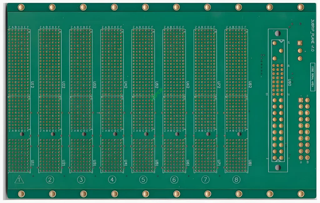
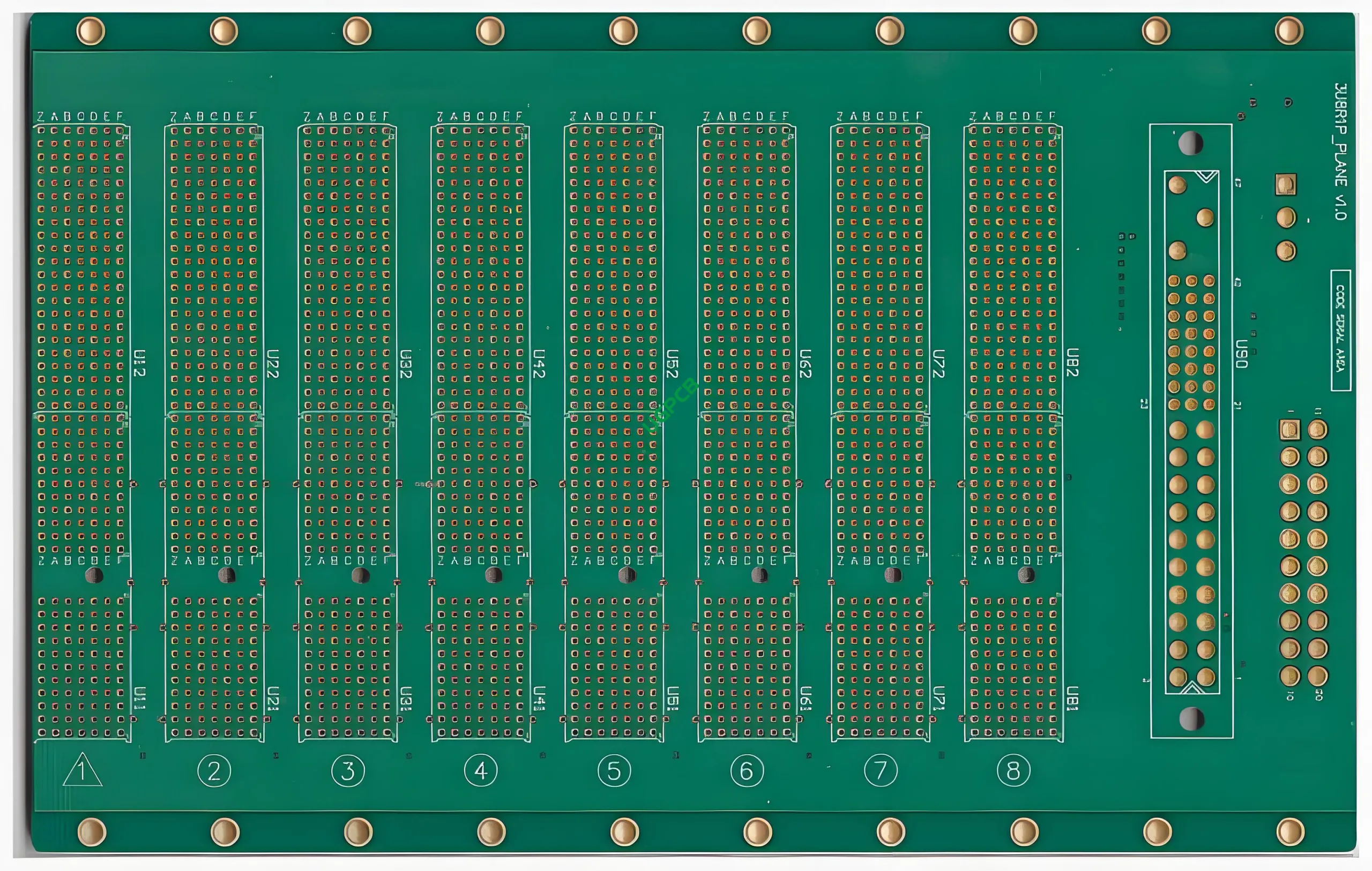
Detalii structurale
The structural details of the 24 Layers Communication Backplane PCB are as follows:
- Număr de straturi: 24 straturi
- Grosime terminată: 2.0mm
- Grosime de cupru: 1Oz
- Lățimea minimă a urmelor: 6mil (0.15mm)
- Spațiu minim între urme: 6mil (0.15mm)
- Tratament de suprafață: Aur de imersiune
Caracteristici și beneficii
The key features and benefits of the 24 Layers Communication Backplane PCB include:
- Interconectivitate de înaltă densitate
- Integritate excelentă a semnalului
- Construcție mecanică robustă
- Performanță fiabilă pe termen lung
- Opțiuni estetice de culoare (Albastru/alb)
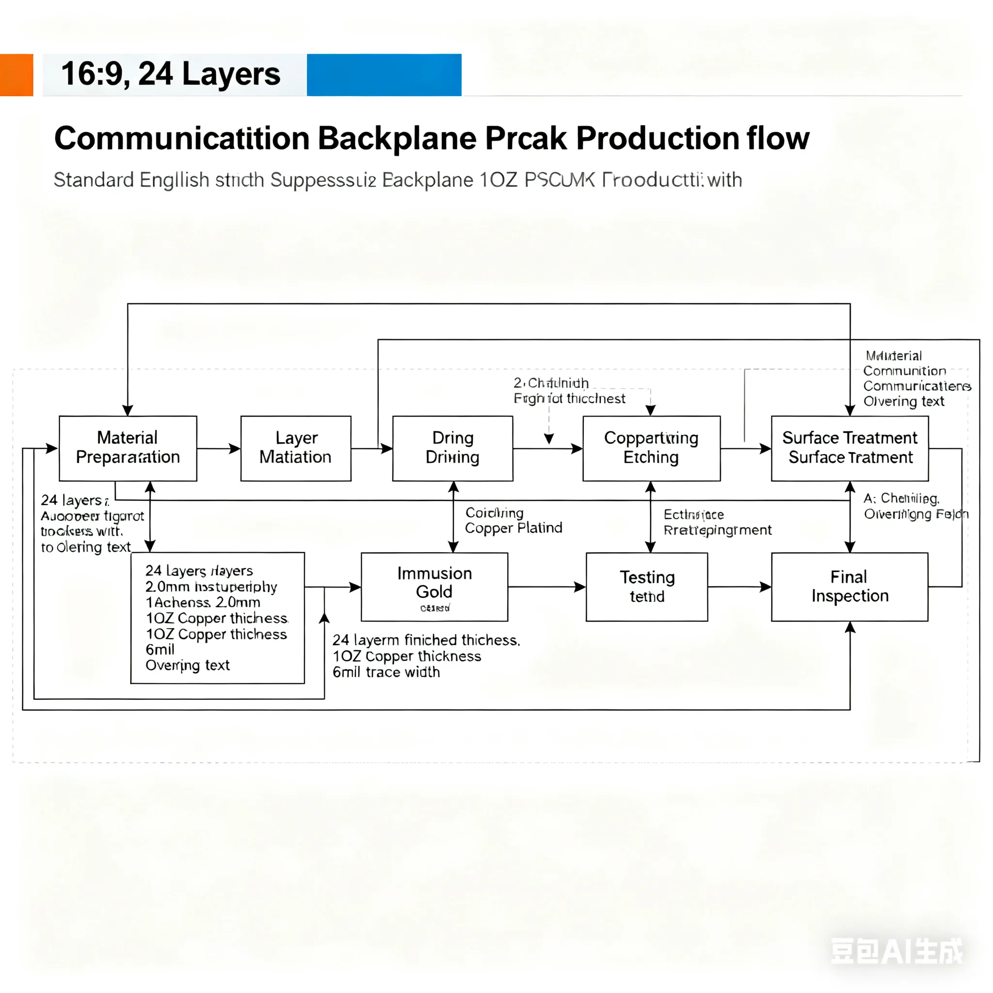
Proces de producție
The production process of the 24 Layers Communication Backplane PCB involves several steps, inclusiv:
- Selectarea materialelor: Choosing high-quality Panasonic M6 material.
- Stivuirea stratului: Aranjând 24 straturi cu precizie.
- Gravură: Înlăturarea excesului de cupru pentru a forma modelele dorite.
- Placare: Aplicarea tratamentului de suprafață a aurului de imersiune.
- Asamblare: Încorporarea PTH -urilor și VIA -urilor pentru interconectări de straturi.
- Testare: Asigurarea că PCB îndeplinește toate specificațiile de performanță.
Cazuri de utilizare

The 24 Layers Communication Backplane PCB is used in various scenarios, ca:
- High-speed data transmission networks
- Telecommunication infrastructure projects
- Advanced networking equipment
- Data center applications requiring high bandwidth
În concluzie, cel 24 Layers Communication Backplane PCB is a sophisticated and reliable component designed to meet the demanding requirements of modern communication systems. Designul său de înaltă densitate, Caracteristici excelente de performanță, and robust construction make it an essential part of any advanced telecommunication setup.


