Heavy Copper PCB Overview
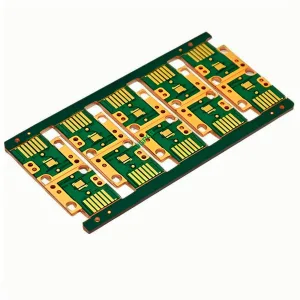
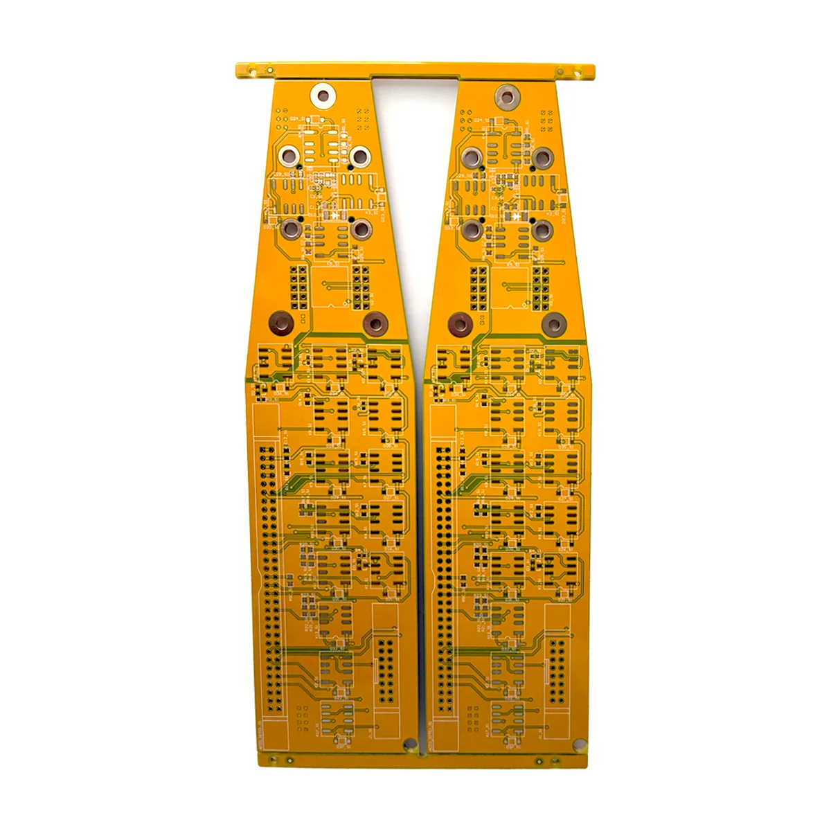
The Heavy Copper PCB is a specialized type of placa de circuit imprimat designed to handle high current applications. It features an increased copper thickness compared to PCB-uri standard, making it ideal for power-intensive electronics. Below is a detailed introduction to this advanced PCB tehnologie.
Clasificare
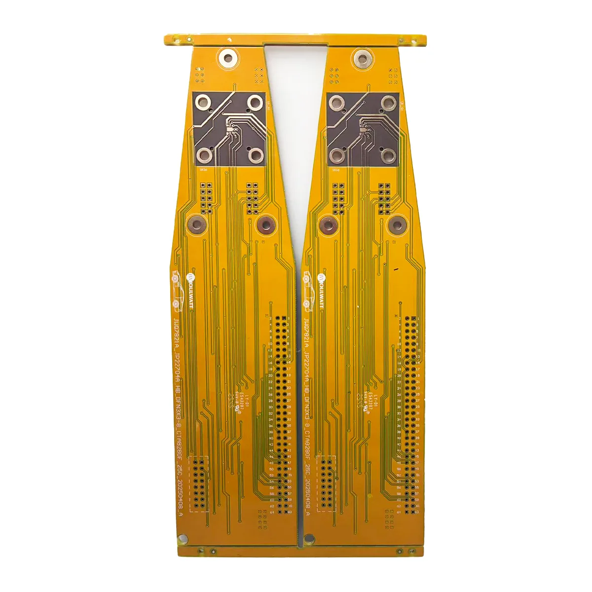
Heavy Copper PCBs are primarily classified based on their copper thickness. Common classifications include 2OZ, 3Oz, 4Oz, up to 6OZ (or 70um and above). Modelul prezentat aici, PCB de cupru greu, offers copper thicknesses of 2OZ and 6OZ, tailored to meet various high-power requirements.
Compoziție materială
The Heavy Copper PCB utilizes Și S1141 as its base material, a high-quality substrate known for its electrical and mechanical properties. The PCB is constructed with 6 straturi, ensuring robust performance and reliability.
Caracteristici de performanță
Heavy Copper PCBs excel in handling high currents due to their thick copper layers. They also offer excellent thermal conductivity, which helps in dissipating heat efficiently. The surface technology used, Aur de imersiune (1-3U), provides a protective coating that enhances corrosion resistance and improves solderability.
Proiectare structurală
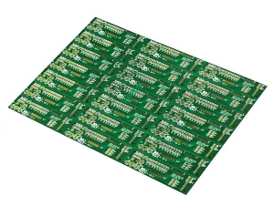
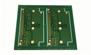
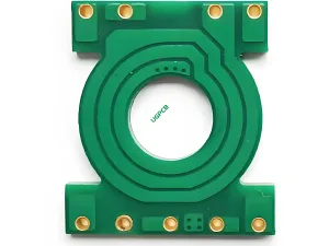
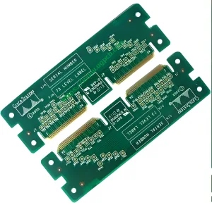
Structural, the Heavy Copper PCB features a board thickness of 2.8mm, oferind o bază solidă pentru componente. The green solder mask color not only enhances visual appeal but also provides insulation and protection against environmental factors. The white silk screen adds to the board’s readability by clearly marking component locations and other essential information.
Caracteristici distinctive
The defining feature of Heavy Copper PCBs is their ability to carry high currents without overheating or experiencing excessive voltage drop. This is achieved through the use of thick copper layers, which also contribute to the board’s overall durability. În plus, the immersion gold surface finish ensures long-term reliability and ease of soldering.
Proces de producție
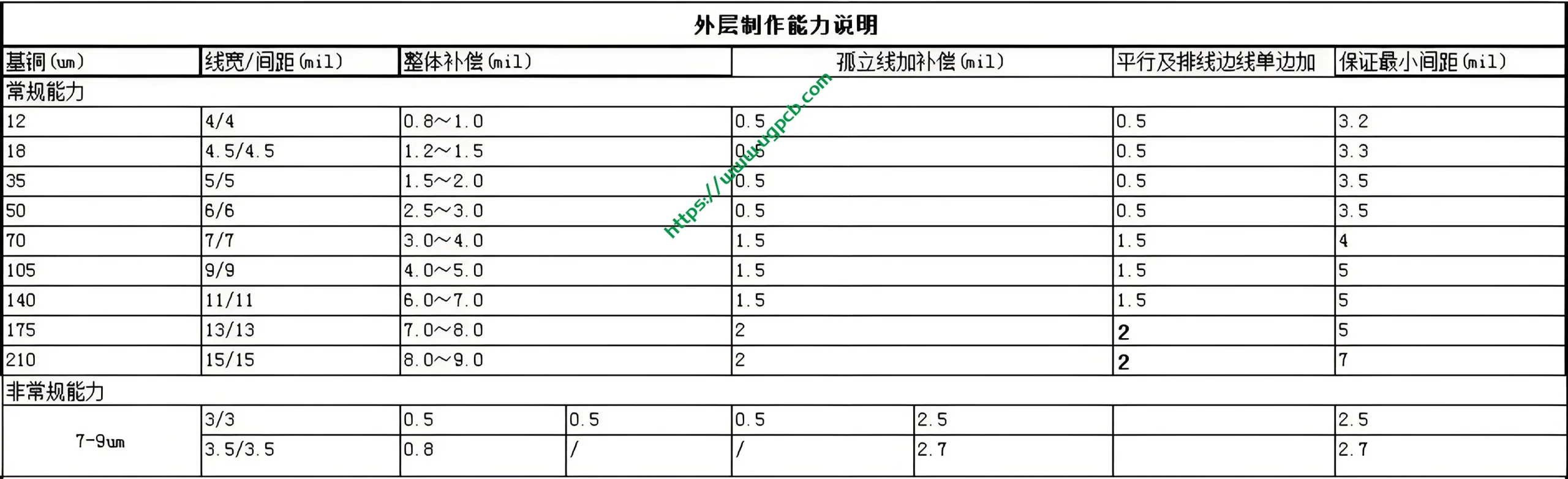
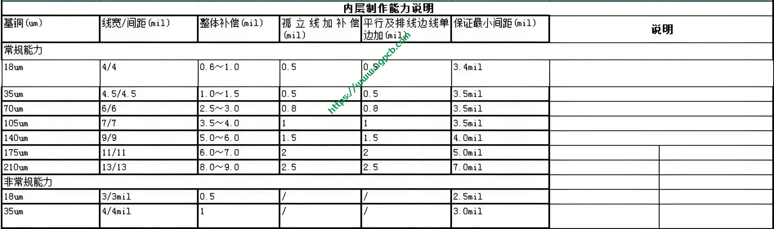
The production of Heavy Copper PCBs involves several precision steps:
- Base Material Preparation: The SY S1141 substrate is prepared and cut to size.
- Laminare de cupru: Thick copper foil is laminated to the substrate using advanced bonding techniques.
- Modelarea circuitului: The desired circuit patterns are etched onto the copper foil.
- Straturi de stivuire și laminare: Multiple layers are stacked and laminated together to form the final PCB structure.
- Forare si placare: Găurile sunt găurite pentru montarea componentelor și interconectarea, urmată de placare pentru a spori conductivitatea.
- Aplicație Mască de lipit: A green soldermask is applied to protect the circuits and provide insulation.
- Serigrafie: White silk screen ink is used to print component labels and other markings.
- Aplicație de finisare a suprafeței: The immersion gold coating is applied to the PCB surface.
- Inspecție finală și testare: The PCB undergoes rigorous inspection and testing to ensure quality and performance.

Scenarii de aplicație
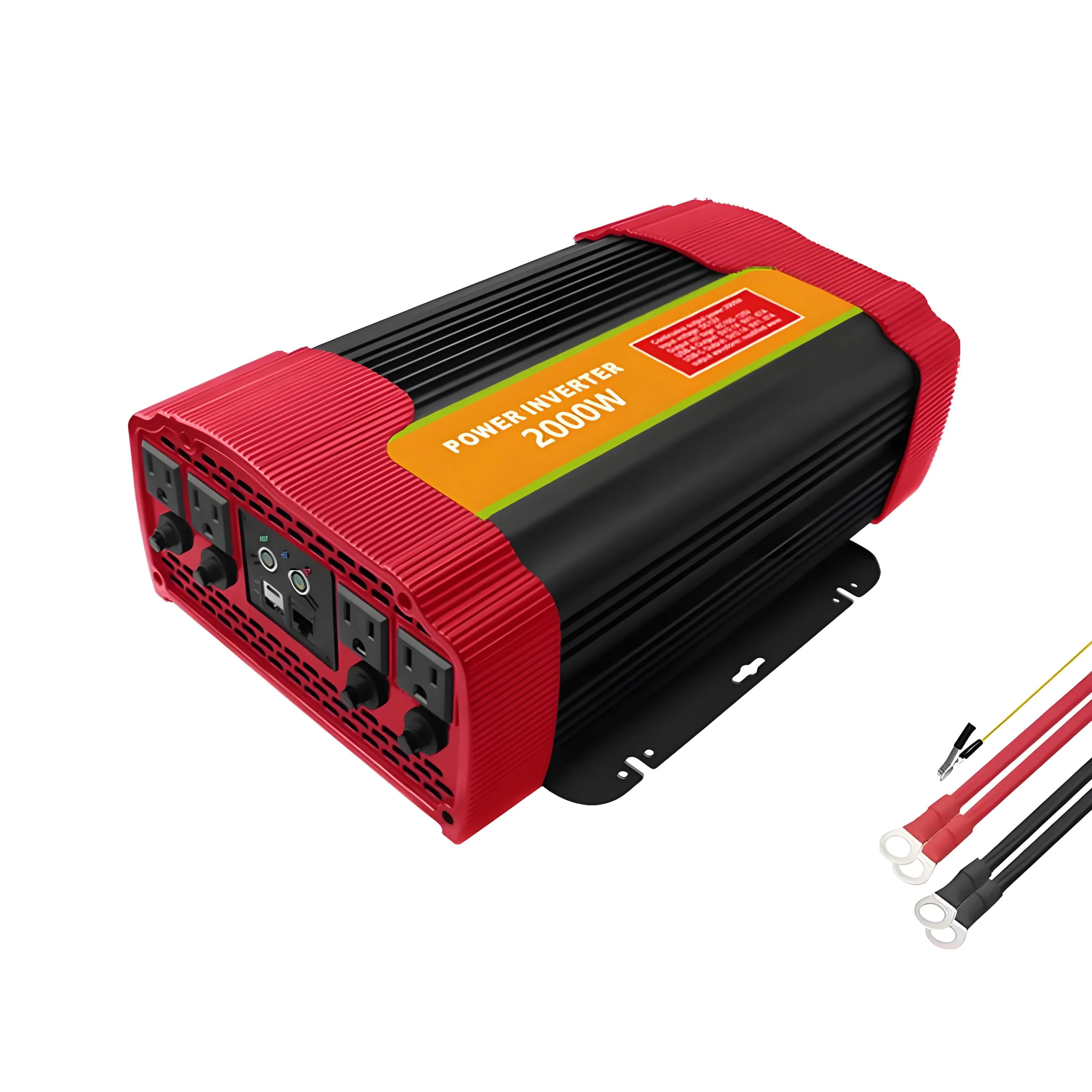
Heavy Copper PCBs are widely used in power converter applications due to their ability to handle high currents and dissipate heat efficiently. They are also suitable for other high-power electronics, such as inverters, controlere de motoare, și sisteme de management al bateriei. În aceste aplicații, Heavy Copper PCBs ensure reliable performance and extended product lifespan.