Why Communication Hardware Demands 6L 2+N+2 HDI PCB Technology
A 5G massive MIMO antenna array packs dozens of RF channels into a single radio unit. A 400G optical transceiver routes 100G PAM4 lanes through a board no larger than a credit card. Standard through-hole PCB-uri multistrat hit a hard wall in these designs. Mechanical drills consume pad real estate on every layer. Routing channels disappear. Signal integrity collapses at multi-gigabit rates.
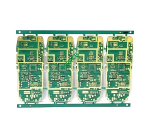
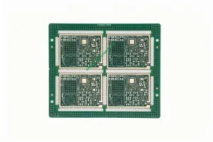
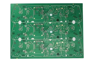
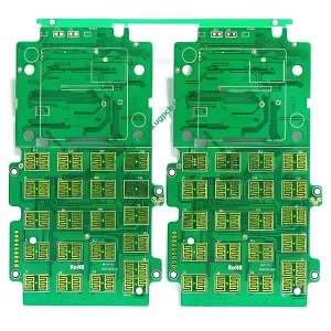
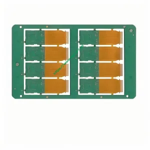
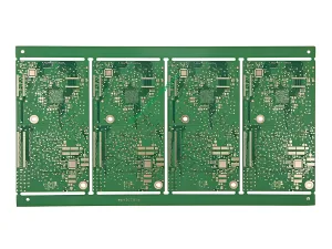
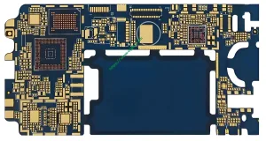
UGPCB’s 6L 2+N+2 HDI communication PCB solves this routing bottleneck. Acest PCB de interconectare de înaltă densitate delivers six functional layers within a 0.8 mm grosime finisata. Susține 0.4 mm pitch BGA escape routing. Laser microvias at 0.1 mm replace mechanical through-holes in the HDI buildup. The ITEQ IT-150 series laminate keeps dielectric loss low enough for 10 GHz-class signals.
This PCB suits 5G small cells, module optice transceiver, routere de bază, and industrial edge gateways. The sections below explain the stackup, stiinta materialelor, Reguli de proiectare, manufacturing flow, and qualification standards behind this PCB building block.

Core specifications at a glance:
- Număr de straturi: 6 straturi, 2+N+2 HDI construction
- Material de bază: ITEQ IT-150 series, halogen-free, mid-Tg
- Grosimea finisata: 0.8 mm
- Greutate de cupru: 0.5 Oz (outer and inner layers)
- Minimum trace / spaţiu: 3 mil / 3 mil (≈ 0.076 mm)
- Minimum laser via diameter: 0.1 mm
- Finisaj de suprafață: aur de imersie + OSP (organic solderability preservative)
- Masca de lipit: verde / alb
What Is an HDI PCB? Decoding the 2+N+2 Stackup
The IPC-2226 definition of HDI and microvia
IPC-2226A defines a microvia as a hole with a diameter of 150 µm or less and a pad density exceeding 20 pads per cm². Un PCB HDI uses these laser-drilled microvias to connect adjacent layers only. Unlike a plated through-hole (PTH), a microvia does not occupy routing space on every layer. This single architectural difference unlocks higher wiring density per unit area.
2+N+2 means two buildup layers per side
The notation “2+N+2” follows the construction terminology in IPC-2226. The two “2”s indicate two microvia layers on each side of the core. The “N” represents the number of core layers. In this 6-layer product, N = 2, so the total layer count is 2 + 2 + 2 = 6.
IPC-2226 classifies 2+N+2 as a Type III HDI construction. Type III requires at least two layers of microvia on one or both sides of the core, and it employs both blind and buried vias. The two buildup steps demand sequential lamination.
Masă 1. 6L 2+N+2 HDI stackup structure
| Strat | Funcţie | Interconectare |
|---|---|---|
| L1 (top) | Semnal / component side | Microvia to L2 |
| L2 | Semnal / sol | Microvia to L1; buried via to L5 |
| L3 | Putere / semnal (miez) | PTH through core |
| L4 | Putere / semnal (miez) | PTH through core |
| L5 | Semnal / sol | Microvia to L6; buried via to L2 |
| L6 (bottom) | Semnal / solder side | Microvia to L5 |
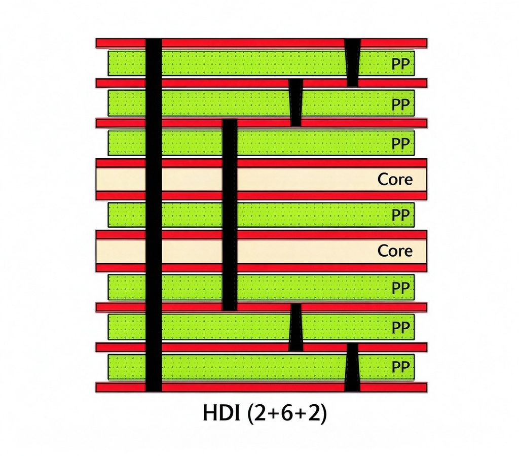
Why communication PCB designers choose 2+N+2 over 1+N+1
A 1+N+1 HDI PCB (Tipul I) offers one microvia layer per side. A 2+N+2 HDI PCB adds a second buildup layer. Într-o 0.4 mm pas, 400-ball BGA, the extra layer roughly doubles the available escape routing channels. This reduces design iterations and protects signal integrity in dense PCBA layouts. Communication PCB designs rarely tolerate the re-spin cost of an underspecified HDI stackup.
ITEQ IT-150 Laminate: The Electrical Foundation of This Communication PCB
Verified dielectric properties
UGPCB builds this HDI PCB on ITEQ’s IT-150 series laminate. The IT-150GXTC data sheet lists Dk = 3.7 și Df = 0.0071 la 10 GHz (53% resin content). The material is halogen-free, mid-Tg (Tg ≥ 150 °C by DSC or TMA), și UL 94 V-0 evaluat. ITEQ designed this laminate family for servers, depozitare, întrerupătoare, and other mid-loss communication PCB applications.
For reference, the IT-150D variant in ITEQ’s IPC technical paper reports Dk/Df ≈ 3.6/0.005 la 10 GHz. Designers should confirm the exact grade with UGPCB before finalizing impedance targets.
Insertion loss impact versus standard FR-4
A simplified dielectric loss estimate follows:
α_dielectric ≈ 2.3 × f × Df × √Dk (dB per unit length, with f in GHz)
Using the IT-150GXTC data sheet values (Df = 0.0071, Dk = 3.7), the dielectric loss at 10 GHz is approximately 0.62 dB per inch. A standard FR-4 with Df ≈ 0.02 and Dk ≈ 4.3 produces roughly 1.95 dB per inch under the same approximation. For a 5-inch differential pair, the laminate choice saves about 6.6 DB of link budget. That margin often separates a compliant 100G lane from a failing one.
IPC-2141A gives the signal propagation velocity as v = c / √Dk. Cu Dk = 3.7, signals travel at approximately 52% a vitezei luminii in vacuum. This value supports tighter intra-pair skew control in high-speed communication PCB routing.
Thermal and environmental reliability
IT-150GXTC carries a UL 94 V-0 cota de inflamabilitate. Its decomposition temperature reaches 390 ° C. la 5% pierdere în greutate, and T260/T288 thermal resistance exceeds 60 minute. These properties allow the PCB to survive lead-free reflow at 260 °C peak without delamination. The halogen-free formulation meets RoHS and REACH restrictions. ITEQ also rates the maximum operating temperature (UL MOT) la 130 ° C..
Design Rules for 6L 2+N+2 HDI Communication PCB
0.1 mm laser microvia geometry
The 0.1 mm laser via is the smallest interconnect feature on this PCB. IPC-2226 treats 0.1 mm as a standard microvia diameter. The dielectric thickness in each buildup layer is approximately 0.075 mm. The resulting aspect ratio is about 0.75:1, well inside the reliable plating window for sequential lamination.
Design the capture pad at 0.25 mm and the target pad at 0.20 mm. La 0.4 mm BGA pitch, adjacent pads leave only about 0.15 mm of clearance. Laser via registration therefore becomes a yield-critical parameter. UGPCB uses laser direct imaging (Ldi) and automated optical alignment to hold registration within ±50 µm, consistent with IPC-6012 Class 3 expectations.
3 mil / 3 mil fine-line routing
The 3 mil trace and space capability places this PCB in the fine-line regime defined by IPC-2226 (≤ 100 µm). These traces run primarily on L1 and L6 to escape microvia arrays and reach BGA pads. O 3 mil wide trace in 0.5 oz copper exhibits roughly 1 mΩ per square of sheet resistance. Pentru 100 Ω differential pairs, adjust the dielectric thickness and pair spacing together. The IPC-2141A microstrip approximation provides a first-order impedance estimate:
Z₀ ≈ [87 / √(εr + 1.41)] × ln[5.98h / (0.8w + t)]
Here h is dielectric thickness in mil, w is trace width in mil, t is copper thickness in mil, and εr is the dielectric constant.
Copper weight and current capacity
Acest PCB folosește 0.5 Oz (≈ 17.5 µm) cupru. IPC-2152 provides the current-carrying capacity reference. O 3 mil wide trace at 0.5 oz supports approximately 0.3 O cu a 10 °C creșterea temperaturii. O 1 mm wide power trace supports approximately 1.2 O under the same conditions. Route high-current rails on inner layers with wider copper areas or parallel traces where the PCBA layout permits.
How UGPCB Manufactures the 6L 2+N+2 HDI PCB
Laminare secvențială: the two-buildup process
The 2+N+2 construction requires two separate lamination cycles. The process proceeds as follows.
Pas 1 — Core fabrication. Start with a 2-layer core (L3/L4). Pattern the inner layers, etch, and apply brown oxide. Drill the buried vias mechanically at 0.15 mm minimum diameter.
Pas 2 — First buildup lamination. Stack one prepreg sheet and one copper foil on each side of the core. Press at 180–200 °C and 300–400 psi. Pattern L2 and L5. Laser-drill the L1–L2 and L5–L6 microvias.
Pas 3 — Second buildup lamination. Add the second prepreg and foil stack. Press again to form L1 and L6. Laser-drill the second-level microvias and plate the copper.
Pas 4 — Outer layer finish. Etch the outer traces, print solder mask and legend, and apply the immersion gold plus OSP surface finish.
Aur de imersiune + OSP: a dual-finish strategy for communication PCB
Aur de imersiune (De acord) deposits 2–5 µm of nickel şi 0.05–0.1 µm of gold on copper pads. It provides a flat surface for fine-pitch BGA attachment and long storage life. OSP applies an organic azole film on selected areas such as test points and non-soldered vias. The combination balances solderability, signal loss, și cost. ENIG protects BGA pads. OSP keeps high-frequency test structures free of metal-induced loss.
Qualification against IPC-6012 Class 3
UGPCB qualifies this PCB to Clasa IPC-6012 3. Clasă 3 requires an average plated hole wall copper thickness of 25 µm, compared with 20 µm for Class 2. Clasă 3 also mandates microsection evaluation on at least one coupon per production lot. The microsection verifies barrel plating thickness, annular ring integrity, and layer registration.
Where the 6L 2+N+2 HDI Communication PCB Delivers Value
5G and 6G radio units
Remote radio units (RRU-uri) and active antenna units (AAU-uri) represent the highest-volume HDI communication PCB application. Massive MIMO arrays integrate dozens of RF chains on a single board. The 2+N+2 stackup supplies the routing channels and controlled impedance those chains require. Indoor small cells and industrial 5G gateways add further demand for compact, high-layer-count PCBA designs.
Optical transceivers and core routers
400G and 800G optical modules route 100G PAM4 lanes across short board spans. At those rates, laminate Df dominates the channel loss budget. The IT-150GXTC data sheet Df of 0.0071 la 10 GHz supports these lanes when paired with appropriate equalization. The 6-layer HDI stackup fits the DSP, driver, and photonic device interconnects into the module footprint.
Satellite communication and industrial IoT
Satellite payloads and ground terminals also rely on HDI PCBs for dense digital and RF routing. Industrial IoT edge gateways operate across wide temperature swings. The halogen-free IT-150GXTC formulation and its 390 °C decomposition temperature provide thermal margin in these environments.
Întrebări frecvente
Î1: How does 6L 2+N+2 HDI differ from a standard 6-layer through-hole PCB?
A standard 6-layer PCB uses mechanical PTHs that pass through every layer. A 2+N+2 HDI PCB uses 0.1 mm laser microvias that connect only adjacent layers. The microvias free routing space on the other layers. This roughly doubles the escape routing capacity in 0.4 mm pitch BGA regions.
Q2: Does IT-150GXTC support 10 Gbps and 25 Gbps signaling?
The data sheet Df of 0.0071 la 10 GHz supports 10 Gbps NRZ links with adequate margin. Pentru 25 Gbps și mai sus, combine the laminate with transmit equalization and receiver CTLE. Confirm the exact IT-150 grade with UGPCB before locking the stackup.
Q3: What is the advantage of immersion gold plus OSP?
ENIG delivers a flat, solderable surface with long shelf life for BGA pads. OSP adds no metal to test points, so it minimizes high-frequency loss there. The dual finish lowers cost without compromising PCBA assembly yield.
Î4: What are the minimum order quantity and lead times?
UGPCB supports prototypes through volume production. Standard lead time for 6L 2+N+2 HDI PCB prototypes is 7–10 business days. Volume production runs 3–4 weeks. Final lead time depends on the Gerber review and stackup confirmation.
Request a Quote and Technical Review
Send your Gerber files or stackup drawing to UGPCB. Our engineering team will return a DFM report and a quotation within 24 ore. We will also recommend stackup adjustments for your specific 5G, optic, or industrial communication PCBA.
Next steps:
- Please send the Gerber files to our online engineering team. We will provide a detailed DFM analysis report and quotation within 24 ore.
- Ask for a stackup review against your impedance and layer-count targets.
- Request a sample to validate IT-150GXTC performance in your design.
📧 E-mail: sales@ugpcb.com
🌐 Site web: www.ugpcb.com
📞 Telefon: +86-135 4412 8719
Data Sources
The technical data and standards cited in this article come from the following sources.
- Corporația ITEQ, IT-150GXTC Data Sheet, Rev. 1.0-20 — Dk = 3.7 la 10 GHz, Df = 0.0071 la 10 GHz, Tg = 150 ° C., Td = 390 ° C., Ul 94 V-0, UL MOT = 130 ° C..
- IPC-2226A, Sectional Design Standard for High Density Interconnect (HDI) Placi imprimate — Type III construction, microvia definition, and 2+N+2 notation.
- IPC-6012F, Specificații de calificare și performanță pentru plăci imprimate rigide — Class 3 average hole wall copper thickness of 25 µm and microsection requirements.
- IPC-2141A, Design Guide for High-Speed Controlled Impedance Circuit Boards — propagation velocity and microstrip impedance approximations.
- IPC-2152, Standard pentru determinarea capacității de purtare a curentului în proiectarea plăcii imprimate — current capacity reference for 0.5 oz copper traces.
- Corporația ITEQ / IPC technical paper, Pierdere scăzută & Novel Halogen-Free Laminates for High Frequency Device Applications — IT-150D Dk/Df ≈ 3.6/0.005 la 10 GHz as a family reference.