

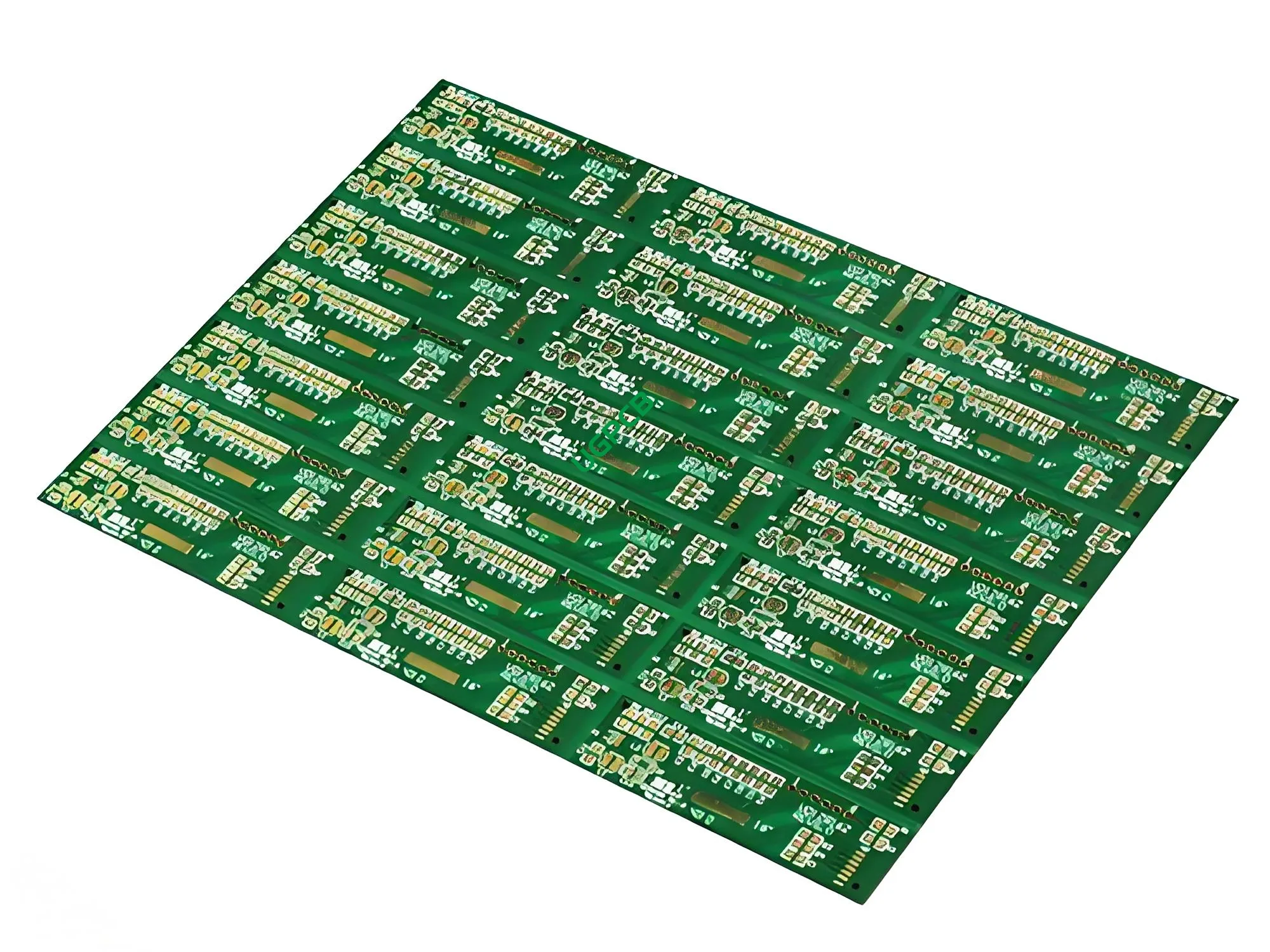
Overview of the P2.9 LED Printed Circuit Board
The P2.9 LED Printed Circuit Board (PCB) is a specialized PCB designed for use with P2.9 LED modules, which are commonly used in high-resolution display applications. This PCB is ideal for creating large, seamless LED displays.
What is a P2.9 LED Printed Circuit Board?
A P2.9 LED Printed Circuit Board is a printed circuit board (PCB) specifically designed to accommodate and connect P2.9 LED modules. The term “P2.9” refers to the pixel pitch of the LED module, which measures 2.9 millimeters between each pixel. This PCB ensures that the LED modules can be interconnected efficiently, providing a stable platform for the electronic components.
Cerințe de proiectare
The design requirements for a P2.9 LED Printed Circuit Board are stringent to ensure its performance and reliability:
- Material: SY1000-2 TG170 FR4, chosen for its excellent electrical and thermal properties.
- Număr de straturi: 6 layers to accommodate the necessary circuitry and signal integrity.
- Culoare: Negru/alb pentru o identificare ușoară și un apel estetic.
- Grosime terminată: 1.0mm to provide structural integrity and durability.
- Grosime de cupru: 1OZ to ensure adequate conductivity and heat dissipation.
- Tratament de suprafață: Aur de imersiune pentru a spori lipirea și rezistența la coroziune.
- Urmare minimă și spațiu: 4mil(0.1mm) Pentru a susține modelele de circuit fine.
- Caracteristică: More pads with small spacing to accommodate the dense layout of P2.9 LED modules.
Cum funcționează?
The P2.9 LED Printed Circuit Board works by providing a platform for various electronic components to be interconnected through conductive pathways. Aceste căi, sau urme, sunt confecționate din cupru și sunt gravate pe tablă. The SY1000-2 TG170 FR4 material ensures that the PCB can withstand the demands of LED display applications, while the immersion gold surface treatment ensures that these traces remain conductive and resistant to corrosion.
Aplicații
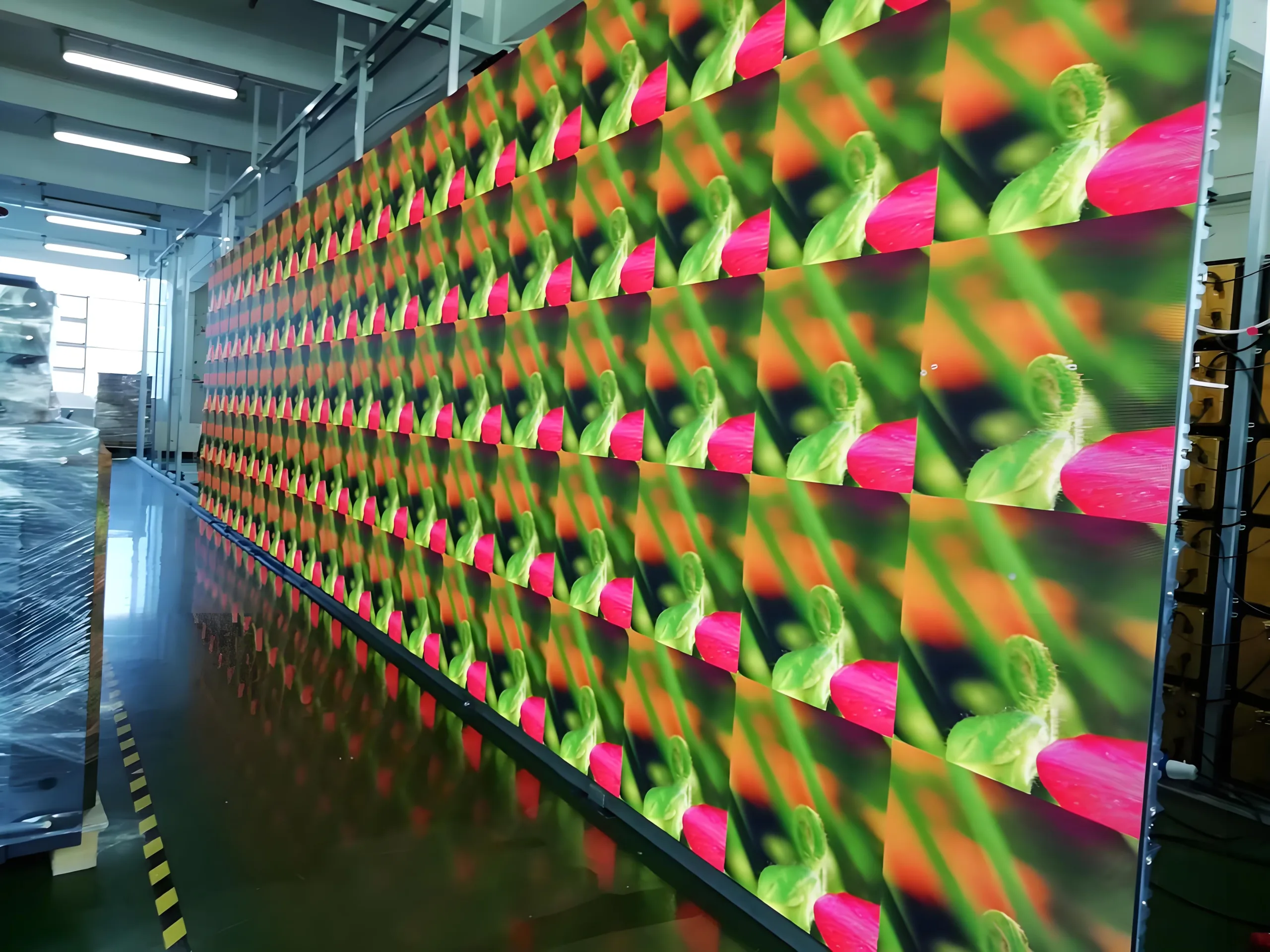
The primary application of the P2.9 LED Printed Circuit Board is in high-resolution LED display systems where it manages and regulates the flow of electrical signals. Aceasta include:
- Indoor and outdoor LED displays
- Digital signage
- Large format video walls
- Event stages and concert screens
Clasificare
Pe baza caracteristicilor și aplicațiilor sale, the P2.9 LED Printed Circuit Board can be classified as a high-density, high-speed digital PCB designed for LED display applications. This classification highlights its capability to handle high-frequency signals and provide stable electrical connections.
Compoziție materială
The core material used in the P2.9 LED Printed Circuit Board is SY1000-2 TG170 FR4, a high-performance composite material known for its excellent mechanical, termic, și proprietăți electrice. This material ensures that the PCB can withstand the demands of LED display applications.
Caracteristici de performanță
The performance characteristics of the P2.9 LED Printed Circuit Board include:
- High signal integrity
- Low signal loss
- Management termic superior
- Rezistență mecanică robustă
- Stabilitatea pe termen lung
Detalii structurale
The structural details of the P2.9 LED Printed Circuit Board are as follows:
- Număr de straturi: 6 straturi
- Grosime terminată: 1.0mm
- Grosime de cupru: 1Oz
- Tratament de suprafață: Aur de imersiune
- Urmare minimă și spațiu: 4mil(0.1mm)
- Caracteristică: More pads with small spacing to accommodate the dense layout of P2.9 LED modules.
Caracteristici și beneficii
The key features and benefits of the P2.9 LED Printed Circuit Board include:
- Interconectivitate de înaltă densitate
- Integritate excelentă a semnalului
- Construcție mecanică robustă
- Performanță fiabilă pe termen lung
- Opțiuni estetice de culoare (Negru/alb)
Proces de producție
The production process of the P2.9 LED Printed Circuit Board involves several steps including:
- Selectarea materialelor: Choosing high-quality SY1000-2 TG170 FR4 material.
- Stivuirea stratului: Aranjând 6 straturi cu precizie.
- Gravură: Înlăturarea excesului de cupru pentru a forma modelele dorite.
- Aplicație de mască de lipit: Applying a solder mask layer to protect the copper traces.
- Placare: Aplicarea tratamentului de suprafață a aurului de imersiune.
- Asamblare: Încorporarea PTH -urilor și VIA -urilor pentru interconectări de straturi.
- Testare: Asigurarea că PCB îndeplinește toate specificațiile de performanță.
Cazuri de utilizare
The P2.9 LED Printed Circuit Board is used in various scenarios such as:
- High-resolution indoor and outdoor LED displays
- Digital signage installations
- Concert and event stages with large video walls
- Retail environments with dynamic advertising screens


