
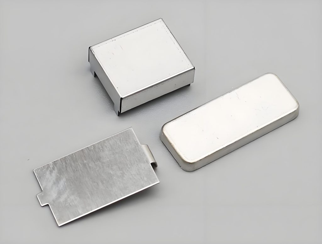
В дизайн печатной платы, engineers often treat a shield can as a simple metal cover. Однако, in 5G communication modules, autonomous driving controllers, and medical imaging equipment, the shield can transforms from an optional cover into a core structure that determines whether a product passes EMC certification. This article analyzes shield can design from three dimensions: теория электромагнитного поля, industry standards, and engineering practice.
1. Shielding Effectiveness: Defining Interference Immunity with Mathematics
The core function of a shield can uses one professional term for precise measurement: Shielding Effectiveness (С). According to IEEE STD-299.1-2013, SE is defined as twenty times the base-10 logarithm of the ratio of incident field strength to transmitted field strength:
SE = 20·log₁₀(E₀ / E₁) (дБ)
Where E₀ is the incident field strength and E₁ is the transmitted field strength. This formula quantifies how much a shield can attenuate electromagnetic waves. Например, SE = 30 dB means the transmitted field strength is about one-thousandth of the incident field. SE = 60 dB corresponds to an attenuation of one part per million.
Practical measurement parameters for shielding effectiveness include test frequency range (100 МГц до 6 ГГц), measurement accuracy (±0.5 dB), and dynamic range (≥80 dB). For core circuits such as RF front-end modules (А, VCO, ЛНА), the SE of a shield can typically requires 60–100 dB.
The physical essence of a shield can follows the Faraday cage principle. When an electromagnetic wave hits a metal cavity surface, the induced surface current generates an opposing electromagnetic field that cancels the incident field. Every opening, gap, or poorly grounded point on the cavity can sharply reduce SE and create a so-called “electromagnetic leak.”
2. Dual Function: Blocking External Interference and Suppressing Internal Radiation
A shield can plays two roles on a печатная плата.
Role one: Block external interference from entering critical circuits. Modules like CPU, Ддр, Flash, WiFi, and Bluetooth are highly sensitive to signal stability. If placed next to a power module, a high-frequency switching circuit, or a strong RF signal, the system may experience occasional bit errors or even a complete crash. Studies show that 90% of EMC problems originate from PCB design defects.
Role two: Suppress internal circuit radiation. DCDC converters, power management ICs, and high-speed clock circuits generate strong electromagnetic radiation during operation. Without proper shielding, their harmonics can couple into antenna or sensor paths and cause the whole product to fail EMI testing. This is the most common reason for certification failure in consumer electronics, медицинское оборудование, and automotive controllers.
3. Рекомендации по проектированию: From Grounding Vias to Resonance Avoidance
Shield can design is not simply “a cover plus solder pads.” You must consider both electromagnetic field integrity and manufacturability.
3.1 Grounding Continuity and Via Array Design
Low-impedance connection between the shield can and the PCB ground plane is fundamental for high shielding effectiveness. According to standard engineering practice, place grounding vias evenly along the inside of the shield frame. Recommended via diameter is 0.3 мм, and adjacent via spacing should be 1–2 mm. At corners and interface points, further reduce spacing to ≤1 mm. The bottom of the shield can should make multi-point contact with the PCB ground plane. Place a ground pad every 5 mm to achieve full 360° seamless grounding.
Кроме того, there must be a complete ground plane directly under the shielded area. Do not route any split lines, signal traces, or power traces across this area, because such paths will weaken the electromagnetic barrier.
3.2 Aperture Constraints and Resonance Avoidance
Ventilation holes, debug ports, and test point openings on a shield can are sometimes unavoidable. According to rectangular waveguide theory, the cutoff frequency for a single round aperture is approximately:
f_c ≈ 170 / дюймовый (ГГц)
Where d is the aperture diameter in mm. From this formula: а 0.8 mm hole will start to lose shielding effectiveness above 21 ГГц. If you reduce the hole diameter to 0.3 мм, the cutoff frequency rises to 56 ГГц, which covers the 5G mmWave band.
You should keep the number of openings to a minimum. Use a honeycomb pattern for better shielding performance. If openings are spaced too far apart, they can create standing wave channels at corresponding wavelengths and cause periodic drops in shielding effectiveness. In one real test of a 5G NR n77 RF module, а 0.5 mm aperture with 1.2 mm spacing caused an 18 dB attenuation drop at 3.8 ГГц.
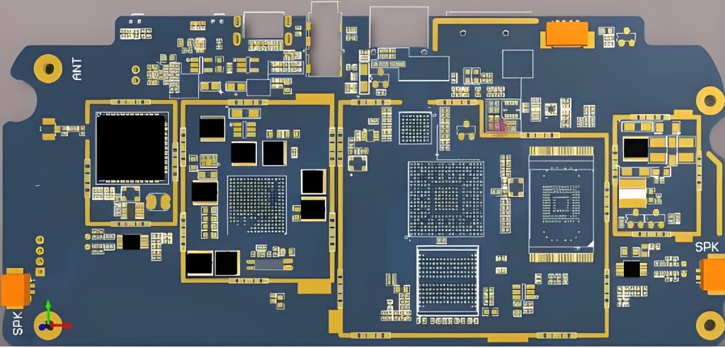
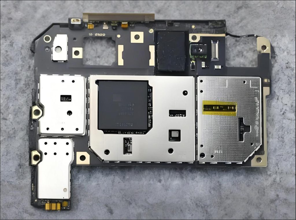
4. Which Modules Need a Shield Can the Most?
Considering interference source levels and sensitivity, the following three module types should be prioritized for shielding.
| Module Type | Typical ICs | Interference Characteristics | Shielding Priority |
|---|---|---|---|
| Power Module | PMU, DCDC, LDO | Strong interference source: high-frequency switching | ★★★★★ |
| Core Module | Процессор, Ддр, EMMC | Sensitive circuit: high immunity required | ★★★★★ |
| Wireless Module | WiFi 6E/7 SoC, Bluetooth | RF signal sensitive | ★★★★★ |
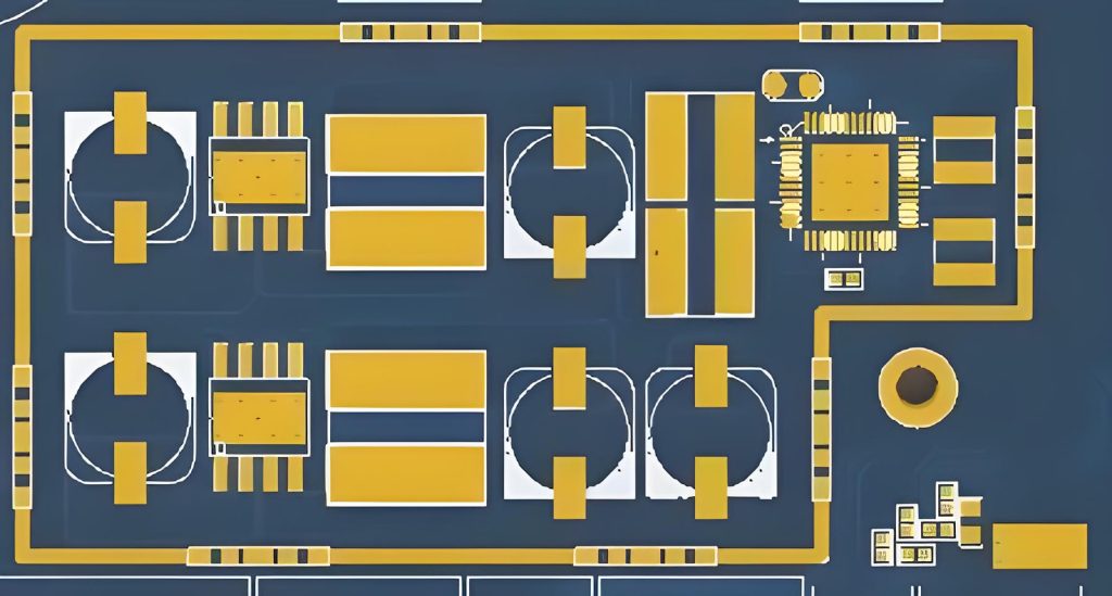
Power modules are both heat sources and interference sources. The high-frequency switching action of the switching power supply generates strong electromagnetic radiation. If a core module experiences interference, the system may show occasional abnormal behavior or even crash and reboot. This failure mode is the least acceptable in any product. Wireless modules are extremely sensitive to interference. You should place the antenna area near the board edge in a relatively clean location, away from complex circuits.
5. Тенденции отрасли: When Shield Cans Meet 5G
The widespread adoption of 5G technology is bringing new challenges to shield can design.
Trend one: Reduced shielding effectiveness in mmWave bands. 5G mmWave bands now reach 28 ГГц. At such frequencies, the skin effect becomes significant. Current concentrates in a layer only about 0.03 mm deep on the conductor surface. Traditional metal shielding layers lose about 40% of their effectiveness. Typical base station tests show that a 28 GHz signal experiences 2.1 dB/cm higher loss on ordinary FR4 material than on high-frequency specialty materials.
Trend two: Strict signal purity requirements for Wi-Fi 6E and the 6 GHz band. Wi-Fi 6E extends operation to 6 ГГц. Wi-Fi 7 not only supports 320 MHz channel bandwidth but also introduces 4096-QAM modulation. Higher frequencies make EMI coupling more severe. Shield can design must upgrade from simple “spatial blocking” to a hybrid approach combining full-band low-impedance grounding and cavity resonance suppression.
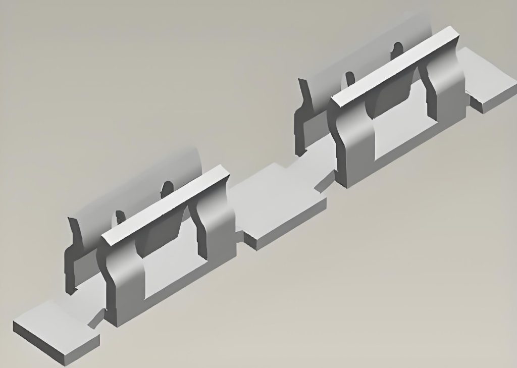
Trend three: Shield assembly moving from manual to SMT automation. Shield clips can be SMT-assembled. They have small size and reduce mold costs. В общем, you can place shield clips with a pitch of about 25 мм. At corners, place clips to help with assembly alignment. Industry data shows that the global market for circuit board EMI shields reached $55.48 million in sales in 2025 and is expected to reach $82.79 million by 2031, with a CAGR of 6.90%. Китай, as the world’s Производство печатных плат hub, has seen the emergence of professional shield can suppliers with precision progressive stamping and fully automated optical inspection. Typical shield can products achieve 30 dB shielding effectiveness at 1 ГГц, flatness ≤0.02 mm, and batch consistency as high as 99.95%.
Заключение
Shield can design may seem like a small detail, but it tests an engineer’s comprehensive understanding of EMI, mechanical structure, процесс, и массовое производство. If you are developing a product with strict EMC requirements, please contact our печатная плата team for a цитировать. Or visit our supplier platform to learn about one-stop печатная плата fabrication and печатная плата assembly services. Truly skilled designers do not treat shield cans as a last-minute fix. Вместо, they consider shielding as a core element from the very beginning of the layout stage.
*Data in this article references IEEE STD-299.1, МПК-2221, GB/T 9254, МЭК 61000-4-21, QYResearch industry reports, and actual measurements from multiple reputable shield can suppliers. Some data comes from 2025–2026 industry white papers and market research reports.*
