
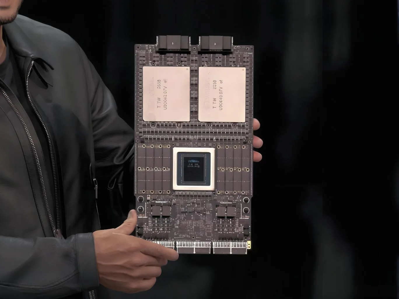
Ортогональная объединительная плата печатная плата является основополагающим компонентом вычислительных кластеров искусственного интеллекта следующего поколения.. Имеет 78-слойную структуру в двухсантиметровом профиле и площадь почти один квадратный метр., он обеспечивает прямое соединение до 576 графические процессоры. Этот плата межсоединений высокой плотности Решение для архитектуры NVIDIA Rubin Ultra расширяет границы традиционного производства электроники, требующие беспрецедентной точности в материалах, процессы, и интеграция.
01 Архитектурный сдвиг: Почему ортогональные объединительные платы заменяют традиционные кабели
Переход к технологии ортогональных объединительных плат является прямым ответом на ограничения медных кабелей в массивных системах искусственного интеллекта.. В конфигурации с высокой плотностью размещения, такой как шкаф NVL576., кабельный подход потребует более 20,000 отдельные кабели, добавление значительного веса, сложность, и точки отказа, при этом также страдает от ухудшения сигнала на расстоянии.
В отличие, а “без кабеля” ортогональная объединительная плата интегрирует межсетевую сеть непосредственно в массивную, многослойная печатная плата. Вычислительные и коммутационные узлы подключаются ортогонально через эту единую плату через вертикально расположенные лотки.. Этот передовая технология печатных плат упрощает процесс сборки, потенциально повышая эффективность за счет над 40%, и решает важную пространственную задачу соединения тысяч компонентов в одной стойке..
02 Граница материаловедения: Дилемма производительности M9 и ПТФЭ
В основе этого многослойного Производство печатных плат проблема заключается в самом материале. Архитектура Rubin предполагает высокоскоростной ламинат класса M9., выбран из-за его исключительных электрических свойств: сверхнизкая диэлектрическая проницаемость (Дк) из 3.0 или меньше и минимальный коэффициент диссипации (Дф) из 0.0007 или ниже. Его коэффициент теплового расширения (КТР) жестко контролируется на ≤7 частей на миллион/°C, что имеет решающее значение для стабильности размеров.
Ключевой инновацией в ламинатах М9 является использование кварцевого волокна. (Q-ткань) вместо стандартного стекловолокна. Несмотря на то, что это обеспечивает превосходные электрические характеристики, это создает огромные Производство печатных плат трудности. Твердость кварцевой ткани резко сокращает срок службы сверла в процессе сверления.. Поэтому производители должны использовать дорогие сверла с алмазным покрытием или системы лазерной абляции., существенное повышение себестоимости продукции.
Для дальнейшей оптимизации электрических характеристик на критически важных путях прохождения сигнала., часто используется гибридный подход. Секции платы могут включать ПТФЭ. (Тефлон), ценится за сверхнизкие потери, несмотря на гораздо более высокий КТР. Устранение значительного несоответствия теплового расширения между этими различными материалами — разница в КТР почти 30х— является серьезным препятствием в ламинирование печатной платы, требующие специализированных связующих пленок и точного контроля процесса для предотвращения расслоения или деформации при термическом напряжении..
03 Расширение производственных ограничений: Бурение, Покрытие, и выравнивание слоев
Физический масштаб и количество слоев ортогональной объединительной платы создают экстремальные Проблемы процесса печатной платы. Толщина доски 1-2 см часто в сочетании с диаметром переходного отверстия >0.2мм приводит к экстремальному соотношению сторон (толщина доски зависит от диаметра отверстия) из 100:1 или больше.
Такое соотношение создает серьезные проблемы для меднения сквозных отверстий.. По мере увеличения соотношения сторон, гальваническому раствору становится экспоненциально труднее течь и равномерно откладывать медь внутри отверстий. Передовой пульсовое покрытие методы необходимы для достижения приемлемой однородности, предотвращение пустот или слабых соединений, которые могут поставить под угрозу надежность.
Более того, поддерживать Целостность сигнала печатной платы на высоких частотах, любая неиспользуемая часть переходного отверстия (называется “заглушка”) должны быть удалены путем точного обратное бурение процесс. Достижение допуска по глубине обратного сверления в пределах ±50 мкм на плате такого размера и сложности — это выдающийся подвиг точной обработки., с участием весьма сложных Сжисс системы и измерительные технологии.
04 Проектирование для повышения производительности: Целостность сигнала и управление температурным режимом
Обеспечение чистой передачи сигнала по 78 слои имеют первостепенное значение. Это требует чрезвычайно жесткого контроль импеданса, с допусками в пределах ± 5%, половина типичного пособия для Стандартные печатные платы. Каждый элемент дизайна — ширина трассы, расстояние, толщина диэлектрика — должна быть тщательно рассчитана и выполнена..
На мультигигабитных скоростях передачи данных, физические эффекты, такие как скин-эффект, где ток течет только по поверхности проводника, увеличивают сопротивление и должны быть учтены при проектировании. Сходным образом, предотвращение перекрестные помехи между плотно расположенными следами требует осторожности многоуровневая конструкция и использование заземляющих пластин для изоляции.
Управление температурой печатной платы является не менее важной задачей совместного проектирования. Медные плоскости помогают распространять тепло, изоляционная природа ламината (с теплопроводностью вокруг 25 W/(м · к)) действует как барьер. Эффективное рассеивание тепла от мощных компонентов, таких как графические процессоры, часто требует интеграции металлических тепловых рамок или холодных пластин непосредственно в корпус. Сборка печатной платы, добавление еще одного уровня сложности механической и тепловой конструкции.
05 Цепочка поставок и рыночные последствия
Появление ортогональных объединительных плат представляет собой значительный сдвиг в ценностях печатная промышленность. Стоимость материала и техническая сложность этих плат относят их к премиум-классу., создание высоких барьеров для входа. Мировые поставки специализированных материалов, таких как кварцевая ткань, ограничены., концентрация производственных мощностей среди нескольких ведущих Поставщики печатной платы.
Для компаний, которые могут это освоить передовая технология печатных плат, возможность существенна. По мере того, как архитектуры серверов искусственного интеллекта развиваются и принимают этот форм-фактор, прогнозируется, что спрос на эти сложные платы будет расти, создание нового высокомаржинального сегмента в сегменте ВЧ материалы для печатных плат и производственный рынок. Это стимулирует инновации во всей цепочке поставок., от производителей ламината до производителей оборудования.
06 Будущее развитие технологии печатных плат
Ортогональная объединительная плата является важной вехой в разработка печатной платы, но это не конечная точка. Промышленность продолжает исследования материалов нового поколения., такие как модифицированные углеводороды и другие смолы с низкими потерями., еще больше увеличить потерю сигнала и скорость передачи данных.
Конвергенция технологий упаковки и печатных плат также ускоряется.. Такие понятия, как встроенный компоненты и печатные платы, подобные подложке (SLP) стирает границы между традиционным производством плат и полупроводниковой упаковкой, стремясь создать все более интегрированные и эффективные системы. Успех в области ортогональных объединительных плат обеспечивает фундаментальный опыт, необходимый для этих будущих достижений..
Освоение ортогональной объединительной платы — это больше, чем просто производственное достижение; это декларация технологических возможностей в эпоху искусственного интеллекта. Это требует плавной интеграции материаловедения., точное машиностроение, и дизайн-мышление на уровне системы. Для Производители печатной платы и их клиенты, решение этих экстремальных задач — это окончательный путь к следующему скачку в вычислительной производительности..
