
A 3dB drop between simulated and measured antenna gain is a familiar nightmare for RF engineers. Your ADS or HFSS simulation shows perfect VSWR and symmetrical radiation patterns. But when you test the prototype with a VNA, the gain drops by nearly half – a 3dB loss means 50% less power.

The root cause is rarely the matching circuit. Вместо, PCB manufacturing quietly eats away antenna efficiency. На частотах миллиметровых волн, current flows only on the conductor surface. Tiny sawtooth-like peaks on the copper surface artificially lengthen the current path. Surface finishes either have gold that is too thin to block lossy nickel underneath, or gold that is too thick and becomes a burden. These three factors together create the huge gap between simulation and real-world performance.
Введение
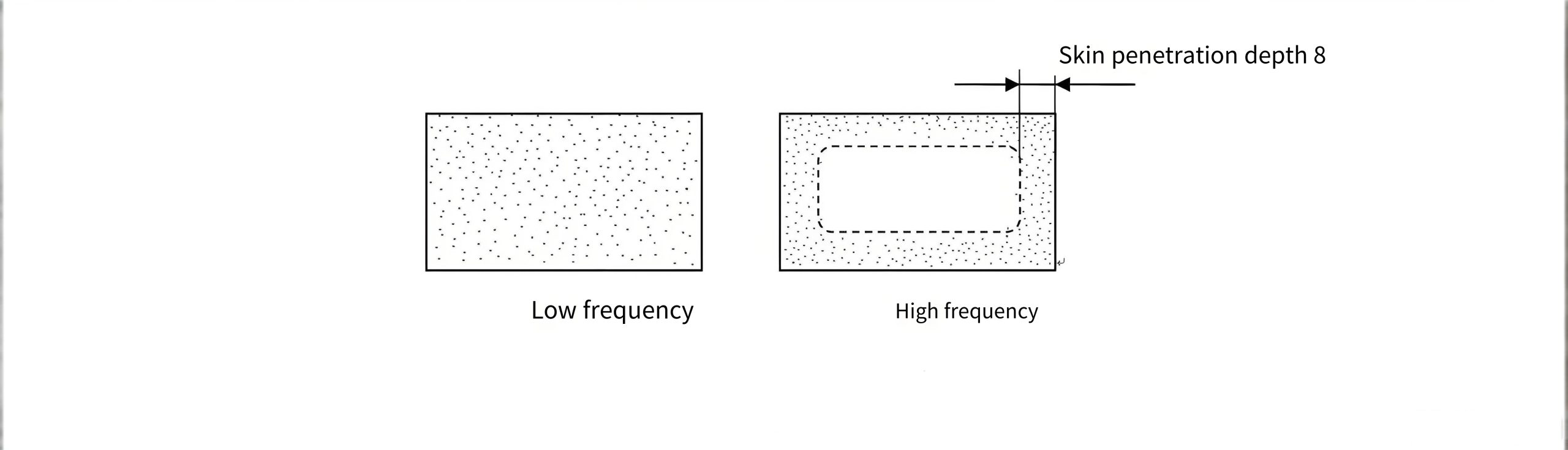
1. Skin Effect: Why High-Frequency Current Takes a Detour
In DC circuits, electrons spread evenly across a wire. Thicker wires mean lower resistance. But at RF and especially millimeter-wave frequencies (2.4ГГц, 5.8ГГц, or 28GHz Ka-band), current flows only on the conductor surface. This is the skin effect.
Current density decays exponentially from the surface inward. The depth where density drops to 1/e (≈36.8%) of the surface value is called the skin depth δ. The formula is:
d = 1 / √(π f μ σ)
Где:
f = frequency (Гц)
μ = conductor permeability (for copper, μ ≈ 4π × 10⁻⁷ H/m)
σ = conductor conductivity (for copper, σ ≈ 5.8 × 10⁷ S/m)
An equivalent form is δ = √(ρ/(являюсь)), where ρ is resistivity. At 25°C, copper resistivity ρ = 1.72 × 10⁻⁸ Ω·m. An engineering approximation δ ≈ 6.62/√f (см) also exists, but it only works under specific conditions.
The table below shows copper skin depth at different frequencies (derived from IPC-2141 standard):
| Частота | 2.4ГГц | 5.8ГГц | 10ГГц | 28ГГц | 60ГГц | 77ГГц |
|---|---|---|---|---|---|---|
| Skin depth | 1.3мкм | 0.8мкм | 0.6мкм | 0.3мкм | 0.33мкм | ~0.2μm |
*Data source: Calculated using copper resistivity ρ = 1.72 × 10⁻⁸ Ω·m.*
When PCB copper thickness (typically 18μm or 35μm) is much larger than the skin depth, the effective resistance depends only on the thin surface layer. That makes copper surface smoothness critical. Industry data shows that every 1dB increase in RF PCB signal loss reduces smartphone download speed by about 15%. Antenna loss directly impacts your product’s competitiveness.
2. Copper Roughness: How Micro-Sawteeth Amplify Loss
Copper foil that looks smooth and shiny to the naked eye appears as rolling “mountain ridges” under a microscope. Higher surface roughness (Rz or Ra) makes the RF current path more tortuous. На частотах миллиметровых волн, every 1μm increase in roughness can add 0.1dB/cm of extra loss.
Insertion loss increases for two reasons. Первый, a rough surface lengthens the current path, which raises effective conductor resistance. Второй, surface bumps distort the local electromagnetic field, causing extra scattering and reflection loss.
IPC-4562A classifies copper foils by roughness. The table below compares different types:
| Тип медной фольги | Surface Roughness Rz | Suitable Frequency Band | Loss Characteristic |
|---|---|---|---|
| Standard electrolytic (STD) | ~5μm | <1ГГц | Базовый уровень |
| Reverse treated foil (РТФ) | 2.5–3.5μm | 2.4Г / 5.8Г | ~40% lower than STD |
| Very low profile (ВЛП) | 1.2–1.8μm | 6–30GHz | ~50% lower than STD |
| Hyper very low profile (ХВЛП) | ≤1.5μm | Mmwave (>30ГГц) | ~60% lower than STD |
Measured case: At 10GHz, RTF foil (Rz≈3μm) has about 0.03dB/inch higher insertion loss than VLP foil (Rz≈1.5μm). Using HVLP foil cuts insertion loss by 0.3dB/inch at 10GHz and keeps impedance fluctuation within ±5% (за IPC-2141A).
At millimeter-wave bands (например, 77GHz automotive radar), conductor loss exceeds dielectric loss and becomes the dominant factor. Our engineering team helped one client reduce the bit error rate of their 77GHz automotive radar PCB from 10⁻⁶ to 10⁻⁹ simply by switching to HVLP copper foil. Choosing the right copper foil is not an option – it is a hard requirement for mmWave antenna design.
3. Толщина золота: ENIG vs. Electroplated Gold – A World of Difference
The choice of PCB surface finish (ENIG vs. electroplated gold) affects RF loss far more than most engineers expect.
СОГЛАШАТЬСЯ (Химическое никель, иммерсионное золото):
Nickel layer thickness: 3–6μm. Gold layer: only 0.05–0.1μm. The problem is the nickel-phosphorus layer in between. Its resistivity is as high as 70 μΩ·cm – 35 times that of pure gold. As frequency rises, skin depth becomes very thin (only 0.33μm at 60GHz). If the gold layer is too thin, the current penetrates through the gold and enters the lossy nickel layer. Measured data show that when gold thickness is only 0.3μm, о 40% of the 60GHz signal current flows in the nickel-phosphorus layer, increasing insertion loss by 2.1dB/cm.
Electroplated Gold (Мягкое золото / Enepic):
Gold thickness can be customized from 0.3μm to 1μm. There is no nickel layer, or the nickel layer is extremely thin. Conductivity is far superior to ENIG. Роджерс’ measured data shows that at 40GHz, ENIG insertion loss is as high as 1.3dB/inch, while UTG (Ultra-Thin Gold) process achieves only 0.75dB/inch. For ENIG, surface roughness Ra must be ≤0.15μm. If Ra exceeds 0.2μm, signal loss at 24GHz degrades significantly.
Practical Selection Guide
- For 2.4G / 5.8G antennas: Prefer electroplated thin gold of 0.5–1μm for feed points and critical traces. Use ENIG only for cost-sensitive designs below 2GHz.
- For mmWave bands (>10GHz): Must use ultra-flat copper foil (Rz. < 0.8мкм) combined with electroplated gold or ENEPIG.
- Толщина меди: Do not blindly pursue 2oz. 35μm copper already provides near-saturated performance above 5.8GHz.
For high-frequency PCB antenna manufacturing quotes or technical support, contact our engineering team for a customized solution.
References
- МПК-2141А, High Frequency Printed Board Design Standard, МПК, 2024.
- IPC-4562A, Metal Foil for Printed Board Applications, МПК.
- Cadence PCB Resources, “Selecting mmWave PCB Materials,» 2025.
- Bittele Electronics, “Manufacturing Technology – Surface Finish Impact,» 2025.
- Jiepei PCB, “High-Frequency PCB Antenna Design Challenges and mmWave Application Breakthroughs,» 2025.
- Anil Kher, “UTG Performs Better Than Other Surface Finishes,»Academia.edu, 2025.
