
В сборке SMT, дефект микронного масштаба может поставить под угрозу качество. Для печатная плата дизайнеры и печатная плата менеджеры по производству, стойкие шарики припоя на контактных площадках компонентов чипа (такие как резисторы и конденсаторы MLCC) являются общей проблемой. Эти дефекты влияют на эстетику и могут вызвать короткое замыкание в требовательных приложениях., угроза надежности продукта. В этом руководстве анализируются пять основных причин появления шариков припоя и дается систематическое описание., МПК-базовое решение для повышения производительности пайки.
Основной механизм: Сжатие пасты и неудачное сдерживание
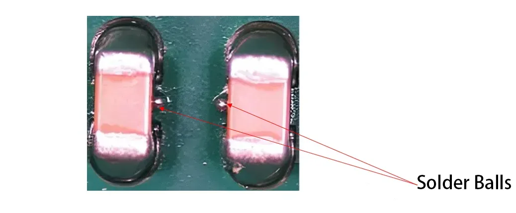
Паяные шарики “побег” скорее, чем “форма.” Во время перекомпоновки, расплавленная паяльная паста не сливается с основным соединением из-за поверхностного натяжения., отделение и комкование по краям подушечки. Пер МПК-А-610, шарик припоя является дефектом, если его диаметр превышает 0,13 мм или если он рискует замкнуть проводники..
Основной причиной является попадание паяльной пасты на паяльную маску во время печати или размещения.. Несмачиваемая паяльная маска предотвращает повторное присоединение пасты к основному соединению., формирование независимых шариков.
Первопричина 1: Проектирование печатных плат “Топография”
дизайн печатной платы это первая защита. Плохая конструкция контактной площадки и паяльной маски создает пути эвакуации.
1. Плотины паяльной маски: Сохранить или удалить?
Традиционные перегородки паяльной маски между соседними чип-площадками предотвращают образование мостов, но создают канавки для улавливания пасты.. Удаление плотины устраняет эту местность., позволяет пасте аккуратно наноситься на подушечку для единого контроля поверхностного натяжения во время оплавления.
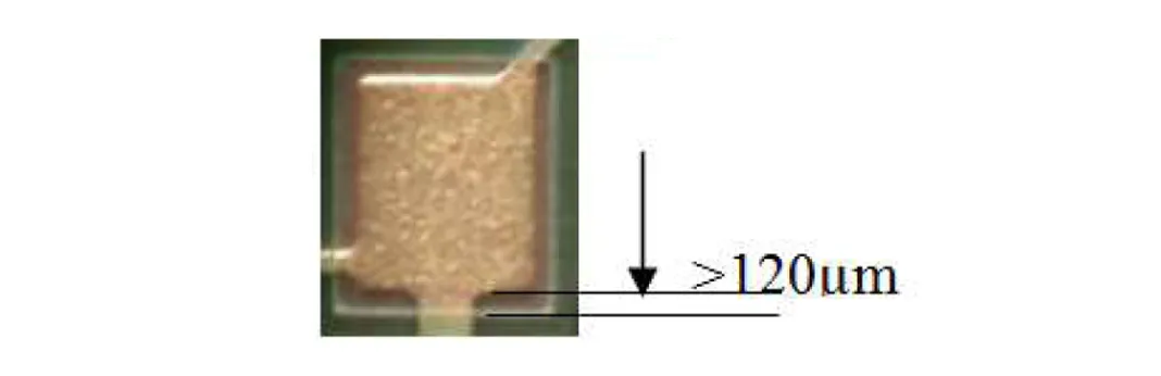
2. Открытие паяльной маски (СМД): Обеспечьте достаточный буфер
SMD должен быть больше, чем медная площадка.. МПК-7351 рекомендует минимум 75 мкм (3мил) односторонний зазор для компонентов чипа, с 120 мкм (5мил) как лучшая практика. Этот буфер компенсирует незначительное смещение паяльной маски., обеспечение контакта пасты только со смачиваемой медью.
3. Управление производственными допусками
Сотрудничайте со своим поставщик печатных плат. Укажите строгие допуски на выравнивание паяльной маски. (обычно ≤50 мкм) и выберите поставщика, способного удовлетворить их потребности в буферной зоне вашего проекта..
Первопричина 2: Трафарет Дизайн “Контроль дозировки”
The трафарет определяет объем и форму пасты.
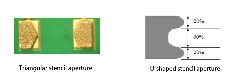
1. Уменьшение объема & Формирование: U-образные/треугольные апертуры
Для 0402 и более крупные компоненты, уменьшить объем пасты. Использование передовых конструкций U-образные или треугольные отверстия. вместо квадратов. Это уменьшает центральный объем и одновременно направляет пасту на концы подушечек., обеспечение достаточного количества припоя при минимизации выдавливания. Это может уменьшить объем пасты на 15-20%.
2. Оптимизация соотношения диафрагмы
Ширина отверстия трафарета обычно составляет 80-90% ширины колодки. Обеспечить Соотношение площади > 0.66 для чистого релиза и точного контроля громкости.
Первопричина 3: Преследование “Нулевой разрыв” в пастообразной печати
Печать определяет начальное размещение пасты.
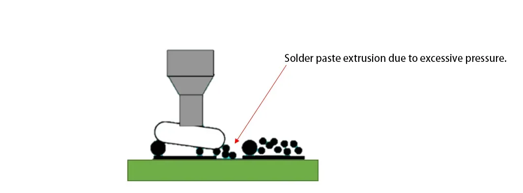
1. Достичь истинного контакта с нулевым разрывом
Любой зазор между трафаретом и печатной платой приводит к вытеканию пасты под давлением ракеля.. Обеспечьте плоскую опорную платформу и оптимальное расположение контактов для равномерной поддержки печатной платы.. Регулярно калибруйте параллелизм станков.
2. Поддерживайте чистоту и выравнивание
Засохшая паста на нижней части трафарета образует зазоры.. Регулярно протирайте нижнюю часть (например, каждый 5-10 платы для компонентов с мелким шагом). Используйте высокоточное выравнивание изображения для идеального совмещения трафарета с контактной площадкой..
Первопричина 4: “Нежный” Размещение компонентов
Размещение может раздавить пасту.
Чрезмерная сила Z или низкая высота установки выдавливают пасту.. Установите высота размещения компонентов к 1/2 к 2/3 высоты постпечатной пасты. Это позволяет детали “целовать” паста без воздействия.
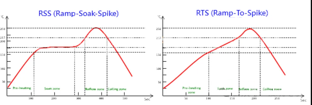
Первопричина 5: Перекомпоновка “Термодинамический” Контроль
Профиль перекомпоновки, особенно разогреть, имеет решающее значение.
1. Избегайте длительного предварительного нагрева и “Горячий спад”
Длинные зоны замачивания могут привести к “горячий спад”: преждевременное испарение флюса/падение вязкости приводит к оседанию пасты и ее растеканию по паяльной маске перед плавлением, приводит к образованию шара.
2. Используйте линейное изменение или линейный профиль.
Сократите или устраните плато замачивания.. Используйте контролируемую линейную рампу от температуры окружающей среды до пика., со скоростью предварительного нагрева 1,0-2,0°С/сек.. Это сокращает время пребывания при низких температурах., ограничивает спад, и обеспечивает синхронное плавление для эффективного поверхностного натяжения.
Точка данных: Пер J-STD МПК/JEDEC-020, для припоя SAC305, цель 60-90 секунды над жидкостью (ИЗ) и пик 235-245°C.. Оптимизируйте наклон предварительного нагрева в рамках этих ограничений..
Заключение: Системный подход к оптимизации
Для решения шариков припоя компонентов чипа требуется системная инженерия подход через дизайн печатной платы, изготовление трафарета, SMT-печать, размещение компонентов, и пайки.
Контрольный список для уменьшения количества шариков припоя:
-
Проектирование печатных плат: Удалены ли перегородки паяльной маски?? Имеются ли отверстия SMD ≥120 мкм??
-
Трафарет Дизайн: Используются ли U-образные/треугольные отверстия?? Правильно ли установлено светосилу?
-
Процесс печати: Часто ли чистят трафарет? Высокая ли точность выравнивания??
-
Программа размещения: Установлена ли высота размещения на 1/2 – 2/3 высоты пасты?
-
Профиль режни: Можете ли вы реализовать линейную рампу с контролируемой скоростью предварительного нагрева??
Для изделий высокой надежности, привлечь профессионала производитель печатных плат для Дизайн для производства (DFM) просмотрите заранее. Опытный партнер EMS может выявить риски и предложить проверенные решения.. Благодаря совместному проектированию и контролю процессов, количество шариков припоя может быть сведено к минимуму до пределов приемлемости IPC, достижение более высокого выхода при первом проходе и превосходной надежности печатных плат.

Мне нравится полезная информация, которую вы предоставляете
ваши статьи. Я добавлю ваш блог в закладки и регулярно заглядываю сюда..
Я почти уверен, что прямо здесь мне расскажут много нового.!
Желаем удачи в дальнейшем!
На самом деле это хорошая и полезная информация. Я доволен, что ты просто
поделился с нами этой полезной информацией. Пожалуйста, держите нас в курсе
такое свидание. Спасибо, что поделились.
Симпатичный! Это было невероятно чудесно
статья. Большое спасибо за предоставление этой информации.
Спасибо за чудесную публикацию! мне конечно было приятно это читать, ты отличный автор.
Я всегда добавлю ваш блог в закладки и обязательно вернусь в будущем..
Я хочу поощрить себя продолжать писать великолепно., иметь
хороший день!
Я пользовался Интернетом более 3 часы сегодня, но я никогда не находил такой интересной статьи, как ваша.
Для меня этого вполне достаточно. С моей точки зрения, если бы все владельцы сайтов и блоггеры делали хороший контент, как, вероятно, и вы, а
Интернет будет намного полезнее, чем когда-либо прежде.
Привет, мне кажется, я увидел, что ты посетил мой блог, поэтому зашел, чтобы вернуть предпочтение?.Я пытаюсь
найти проблемы для улучшения моего веб-сайта!Я полагаю, можно использовать несколько ваших
идеи!!
Я впервые захожу сюда, и мне действительно приятно читать все в одном месте..
After looking at a few of the articles on your web page, I honestly appreciate your technique
of writing a blog. Isaved it to my bookmark website list and will be
checking back soon. Please visit myy website too annd let me know your opinion.