
В современном производстве электроники, технологические дефекты в печатная плата (Печатная плата в сборе) может привести к снижению надежности продукта, увеличение производственных затрат, и даже провалы проектов. Статистика показывает, что дефекты процесса PCBA составляют более 30% ранних сбоев в электронных продуктах, проблемы с паяными соединениями и дефекты покрытия являются основными типами неисправностей. В этом подробном руководстве систематически анализируются десять типичных дефектов процесса PCBA Manufacturing— от шероховатостей покрытия и частиц меди до растрескивания паяных соединений BGA — и обеспечивает стандарт МПК-соответствие, проверенные в боевых условиях решения, помогающие инженерам повысить качество и надежность продукции.
1. Шероховатость покрытия: Невидимый убийца однородности поверхности
Шероховатость покрытия – распространенный дефект Производство печатных плат, характеризуются неровными краями или зернистой текстурой поверхности. Шероховатость кромок часто возникает из-за чрезмерного тока, вызывающего неравномерность покрытия., в то время как полная шероховатость плиты часто возникает из-за недостаточного содержания отбеливателя в условиях низких температур или неправильной подготовки плиты к доработке..
Решения:
- Отрегулируйте параметры покрытия: Уменьшите плотность тока и откалибруйте амперметры для обеспечения стабильного выходного сигнала..
- Оптимизация использования добавок: Добавляйте отбеливатели при низких температурах для улучшения однородности..
- Усиление предварительной обработки: Тщательно очистите ремонтные доски от загрязнений и оксидов..
По стандартам МПК, высококачественные печатные платы должен поддерживать допуск по толщине меди ≤5%. Шероховатость покрытия часто превышает 10% отклонение, критически влияет на токопроводящую способность.
2. Медные частицы на поверхностях печатных плат: Микрозагрязнения в технологической цепочке
Частицы меди проявляются в виде прилипших медных зерен к поверхности платы., происходящие из таких источников, как высокая жесткость в щелочной обезжиривающей воде, сбои в системе фильтрации, загрязненные активаторы в меднении, или неполная очистка во время передачи изображения.
Стратегии смягчения:
- Улучшите обслуживание фильтров: Регулярно заменяйте фильтрующие элементы для поддержания чистоты ванны..
- Оптимизируйте последовательность стирки: Обеспечьте тщательную промывку после переноса изображения и сведите к минимуму время хранения панели..
- Контролировать параметры ванны: Контролируйте содержание меди и кислотность, использование фосфорированных медных анодов с равномерным распределением.
3. Покрытие Питтинг: Тихий убийца пятнистой обшивки
Ямки в покрытии выглядят как пятнистые пустоты на поверхности печатной платы., вызвано загрязнением вешалок в результате ненадлежащей чистки, необслуживаемое оборудование для обработки изображений, или жесткая вода в процессах предварительного покрытия.
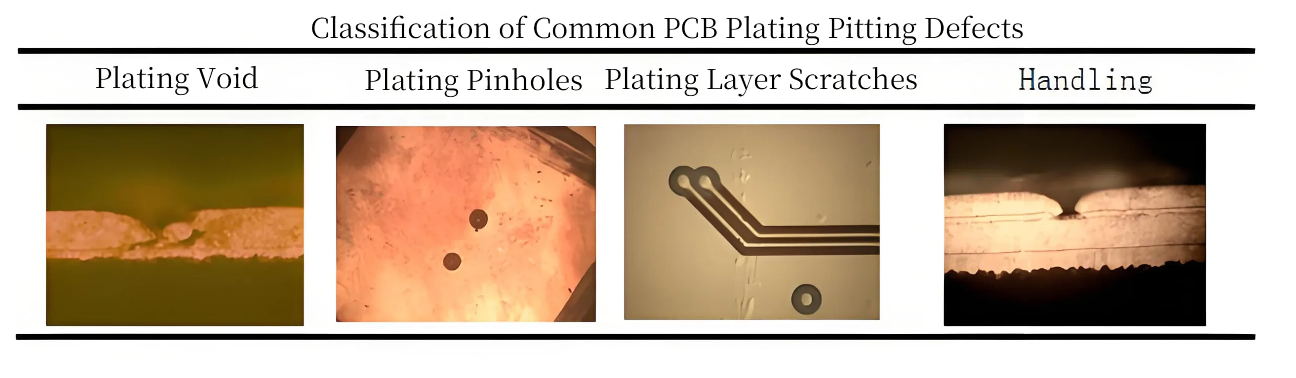
Решения:
- Внедрить протоколы глубокой очистки медных вешалок..
- Запланируйте регулярное техническое обслуживание оборудования для обработки изображений, чтобы обеспечить чистоту разработки..
- Используйте деионизированную воду при предварительном нанесении покрытия и своевременно заменяйте изношенные покрытия подвесок..
4. Побеление поверхности и несоответствие цвета: Визуальные дефекты, имеющие множество причин
Побеление поверхности и изменения цвета возникают из-за неравномерного перемешивания воздуха, вызывающего изменения толщины покрытия., негерметичные фильтр-насосы, загрязненные хлопковые фильтры, несбалансированные концентрации микропротравливателя, плохое качество воды, или неисправные анодные соединения.
Меры по улучшению:
- Отрегулируйте положение распределителя воздуха для равномерного перемешивания..
- Замените квалифицированный фильтрующий материал для контроля органических загрязнений..
- Оптимизация процессов микротравления, улучшить качество воды, и проверьте анодные соединения.
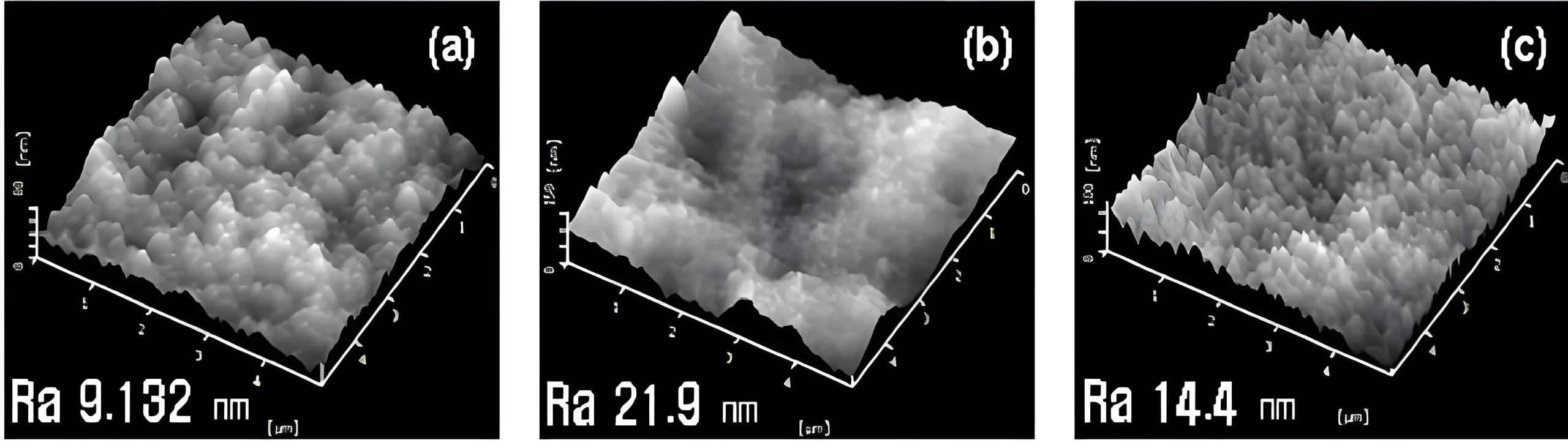
Фигура: Проверка качества плат PCBA под микроскопом с большим увеличением выявляет шероховатости покрытия и частицы меди — критические дефекты, требующие внимания..
5. Дефекты пайки сквозных устройств: Проблемы надежности
Дефекты пайки THD, такой как 8.7% ложная пайка в промышленных платах управления, вытекают из трех основных проблем:
- Материальные факторы: Изменения плотности переплетения стекловолокна вызывают неравномерное распределение тепла..
- Факторы процесса: Неадекватное температурное профилирование при ручной доработке.
- Факторы проектирования: Соотношения сторон (диаметр отверстия/диаметр штифта) ниже IPC 1.5 рекомендация.
Протоколы оптимизации:
- Динамический контроль температуры: Отрегулируйте температуру паяльника в зависимости от температуры стеклования печатной платы. (Тг).
- Средства для смачивания: Используйте не требующий очистки флюс с рейтингом ROL1. “вторичное смачивание” методы.
- Управление процессом: Внедрить трехзонный контроль температуры и отслеживание материалов..
Пост-реализация, скорость заполнения припоя подскочила с 68% к 93%, термоциклирование (-40° C ~ 125 ° C.) достигнуты проходные баллы 100%, и время переделки сократилось с 4.2 к 1.8 минут на единицу.
6. HDI «слепые» переходные отверстия и отказы контактных площадок: Риски высокой плотности надежности
Доски HDI использовать глухие переходные отверстия и изящную укладку для компактных конструкций, но вводить такие риски, как:
- Слепой через надежность: Допуск на лазерное сверление должен оставаться в пределах ±0,02 мм, чтобы предотвратить перекос..
- Пустоты в стенках отверстий: Дисбаланс pH или недостаточное количество активаторов во время химического меднения..
- Недостаточная толщина меди: IPC требует ≥20 мкм для стенок ПТГ, но тонкие участки сохраняются.
Решения:
- Мониторинг толщины в режиме реального времени с помощью встроенных лазерных микрометров (Допуск ±1 мкм).
- Создание баз данных совместимости для систем пайка-флюс-подложка..
- Развертывание датчиков окружающей среды (температура/влажность/ЛОС) с порогами автоматического оповещения.
7. Краевые дефекты процесса: Недооцененные источники цепных реакций
Краевые дефекты (картавит, несовпадение отверстий инструмента, расслаивание) повысить общий уровень дефектов на 10-15%. Средние показатели по отрасли показывают 2.2% процент дефектов по проблемам, связанным с краями, с последствиями, включая:
- Несовпадение отверстий инструмента >0.1уменьшение мм СМТ точность размещения до 0,2 мм (стандартный: 0.1мм).
- Расслоение кромок, ослабляющее структурную целостность за счет 30% и увеличение затухания сигнала 15-20%.
- Заусенцы, вызывающие риск паяльных перемычек и повреждающие сопла для захвата и установки..
Комплексная система управления UGPCB:
- Снятие стресса: Акклиматизируйте субстраты при 25±1°C и относительной влажности 50±5% в течение 12 часы.
- Прецизионное сверление: 0.003станки с точностью до мм и базой данных толщины-скорости.
- Полная отслеживаемость: Интеграция MES для отслеживания дефектов в режиме реального времени.
Эти меры снизили количество дефектов кромок до <0.1%, намного ниже 2.2% Среднее значение в отрасли.
Фигура: Микроскопия дефектов кромок выявляет несоосность инструмента и заусенцы, влияющие на точность поверхностного монтажа..
8. Растрескивание паяных соединений и выход компонентов из строя: Двойные отказы материала и процесса
Растрескивание паяного соединения, критический дефект печатной платы, часто возникает из-за коррозии слоя никеля во время нанесения покрытия ENIG. Окисленный никель образует с припоем неоднородные ИМС., приводящие к трещинам на границе раздела IMC-никель.
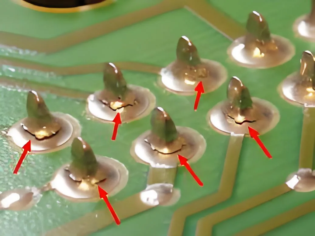
Улучшения процесса:
- Контроль фосфора: Сократите срок службы ванны химического химического никеля для увеличения содержания фосфора. (диапазон высокого P).
- Толщина никеля: Поддерживайте толщину ≥4 мкм, чтобы минимизировать точечную коррозию..
- Толщина золота: Ограничение до ≤0,1 мкм с уменьшенным временем погружения.
9. Неисправности паяных соединений BGA: Микротрещины и концентрация напряжений
BGA-соединения (0.4мм шаг, 0.2высота мм) склонны к микротрещинам при вибрации или термическом ударе. Сервер ИЧР случай показал 300% повышение сопротивления, поствибрационные испытания.
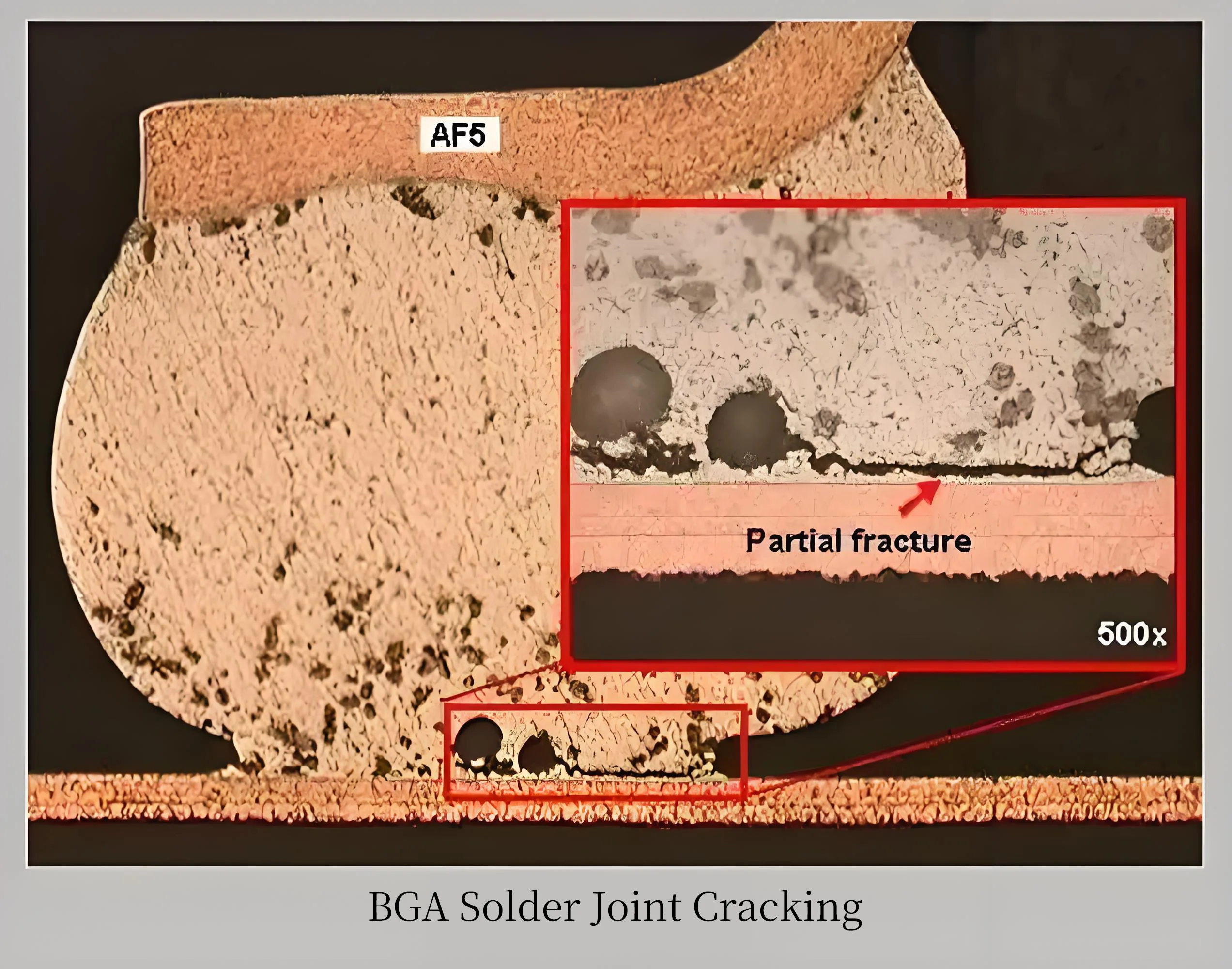
Решения:
- Оптимизация макета: Избегайте неправильного размещения винтов радиатора, вызывающих нагрузку на BGA..
- Контроль изгиба: Сведите к минимуму повторное сгибание, чтобы предотвратить подъем колодки..
- Подбор материалов: Выберите подложки/припой с соответствующим КТР. (например, высокий Tg FR-4 при 8 ppm/°C по сравнению с. стандартное 15 ppm/°C).
10. Неадекватная тепловая конструкция: Кризис компонентов при высокой температуре
Отказ компонентов, вызванный перегревом, является распространенным явлением.. Запатентованный “плата слепого монтажа со встроенным радиатором” улучшает тепловые характеристики за счет внутренних полостей и высокоэффективных радиаторов, быстро рассеивает тепло и снижает риск термического повреждения.
Инновационные конструктивные особенности:
- Тепловые полости усиливают теплообмен между радиатором и платой и общее охлаждение.
- Радиаторы поглощают и рассеивают тепло печатной платы., с воздушным потоком, эффективно отводящим тепло.
Сводная таблица для справки:
| Тип дефекта | Среднее по отрасли. | Улучшенная ставка | Ключевые параметры управления |
|---|---|---|---|
| Краевые дефекты | 2.2% | 0.1% | Точность сверления 0,003 мм, 12ч акклиматизация |
| Ложная пайка THD | 8.7% | 0.9% | Соотношение сторон ≥1,5, трехзонный контроль температуры |
| Отверстие в стене Медь | – | МПК ≥20 мкм | Допуск по толщине ± 1 мкм |
| Скорость заполнения припоя | 68% | 93% | Динамический профиль: 280°C/3 с + 380°С/2с |
Систематический контроль и предотвращение процессов могут уменьшить большинство дефектов печатных плат.. Партнерство с опытными поставщиками и внедрение надежных систем качества являются ключом к повышению надежности печатных плат.. Для высоконадежных решений PCBA и технических консультаций, контакт мы сегодня.

немного действительно интересной информации , хорошо написано и широко доступно пользователю.