
лљ л╝лЙлйЛѓл░лХлйл░ЛЈ л┐л╗л░Лѓл░ лблЙл╗лйлх, ЛЄлхл╝ л▒ЛЃл╝л░л│л░, Лѓлхл┐лхЛђЛї ЛЈл▓л╗ЛЈлхЛѓЛЂЛЈ л║ЛђлИЛѓлИЛЄлхЛЂл║лИл╝ л┐лЙл╗лхЛѓлЙл╝ л▓ л│л╗лЙл▒л░л╗ЛїлйлЙл╝ ЛѓлхЛЁлйлЙл╗лЙл│лИЛЄлхЛЂл║лЙл╝ л║лЙлйл║ЛЃЛђЛЂлх. лъЛѓ ЛЂлхЛђл▓лхЛђлЙл▓ лИЛЂл║ЛЃЛЂЛЂЛѓл▓лхлйлйлЙл│лЙ лИлйЛѓлхл╗л╗лхл║Лѓл░ л┤лЙ ЛЃл╝лйЛІЛЁ ЛѓЛђл░лйЛЂл┐лЙЛђЛѓлйЛІЛЁ ЛЂЛђлхл┤ЛЂЛѓл▓, лЋл│лЙ л┐ЛђлЙлИлил▓лЙл┤лИЛѓлхл╗ЛїлйлЙЛЂЛѓЛї лйл░л┐ЛђЛЈл╝ЛЃЛј лЙл┐Лђлхл┤лхл╗ЛЈлхЛѓ ЛЃЛЂл┐лхЛЁ лИл╗лИ ЛЂл▒лЙл╣ ЛЇл╗лхл║ЛѓЛђлЙлйлйЛІЛЁ л┐ЛђлЙл┤ЛЃл║ЛѓлЙл▓.
лњ ЛѓлхЛЂЛѓлЙл▓лЙл╣ л╗л░л▒лЙЛђл░ЛѓлЙЛђлИлИ UGPCB, лўлйлХлхлйлхЛђЛІ Лђл░лил╝лхЛЅл░ЛјЛѓ лйлхл┤л░л▓лйлЙ л┐ЛђлЙлИлил▓лхл┤лхлйлйЛІл╣ ЛЂлхЛђл▓лхЛђ лўлў л┐лхЛЄл░Лѓлйл░ЛЈ л┐л╗л░Лѓл░ л▓ -55 ┬░ C Extreme Cold Environment, лил░Лѓлхл╝ л▒ЛІЛЂЛѓЛђлЙ л┐лхЛђлхлйлхЛЂЛѓлИ лхл│лЙ л▓ л║л░л╝лхЛђЛЃ л▓ЛІЛЂлЙл║лЙл╣ Лѓлхл╝л┐лхЛђл░ЛѓЛЃЛђЛІ 125 ┬░ C л┐лЙЛЂл╗лх 30 ЛЂлхл║ЛЃлйл┤ЛІ. лГЛѓлЙЛѓ Лђлхлил║лИл╣ ЛєлИл║л╗ л┐лЙл▓ЛѓлЙЛђЛЈлхЛѓЛЂЛЈ 1,000 лњЛђлхл╝ЛЈ-лЙл▒лхЛЂл┐лхЛЄлхлйлИлх л║л░лХл┤ЛЃЛј ЛЂЛЁлхл╝ЛЃ л╝лИл║ЛђлЙлйлйлЙл│лЙ ЛЃЛђлЙл▓лйЛЈ л┐лЙл┤л┤лхЛђлХлИл▓л░лхЛѓ ЛЂЛѓл░л▒лИл╗ЛїлйлЙЛЂЛѓЛї ЛЂлИл│лйл░л╗л░ л▓ ЛЇл║ЛЂЛѓЛђлхл╝л░л╗ЛїлйЛІЛЁ ЛЃЛЂл╗лЙл▓лИЛЈЛЁ.
“лЮл░Лѕ л┐ЛђлЙлхл║Лѓ ЛЄЛЃЛѓЛї лйлх л┐ЛђлЙл┐ЛЃЛЂЛѓлИл╗ ЛЂл▓лЙл╣ л║Лђл░л╣лйлИл╣ ЛЂЛђлЙл║ лИли -лил░ лИлйЛѓлхЛђЛёлхЛђлхлйЛєлИлИ ЛЂлИл│лйл░л╗л░ PCB!” лЙл┐л╗л░л║лИл▓л░л╗л░ ЛѓлхЛЁлйлЙл╗лЙл│лИЛЄлхЛЂл║ЛЃЛј л║лЙл╝л┐л░лйлИЛј R&D лћлИЛђлхл║ЛѓлЙЛђ. лА ЛЃЛЄлхЛѓлЙл╝ л║лЙл╝л┐ЛїЛјЛѓлхЛђлйлЙл╣ л▒ЛЃл╝л░л│лИ лўлў лИ Лђлхл▓лЙл╗ЛјЛєлИлхл╣ л▓ ЛЇл╗лхл║ЛѓЛђлЙлйлйЛЃЛј л░ЛђЛЁлИЛѓлхл║ЛѓЛЃЛђЛЃ лИлйЛѓлхл╗л╗лхл║ЛѓЛЃл░л╗ЛїлйлЙл│лЙ ЛѓЛђл░лйЛЂл┐лЙЛђЛѓлйлЙл│лЙ ЛЂЛђлхл┤ЛЂЛѓл▓л░, лњЛІЛЂлЙл║лЙл║л░ЛЄлхЛЂЛѓл▓лхлйлйлЙлх л┐ЛђлЙлИлил▓лЙл┤ЛЂЛѓл▓лЙ лЪлЦлЉ л┐ЛђлЙЛЁлЙл┤лИЛѓ л▒лхЛЂл┐ЛђлхЛєлхл┤лхлйЛѓлйЛЃЛј ЛѓлхЛЁлйлЙл╗лЙл│лИЛЄлхЛЂл║ЛЃЛј ЛѓЛђл░лйЛЂЛёлЙЛђл╝л░ЛєлИЛј лИ л║лЙлйл║ЛЃЛђлхлйЛєлИЛј лил░ л╝лЙЛЅлйлЙЛЂЛѓЛї.
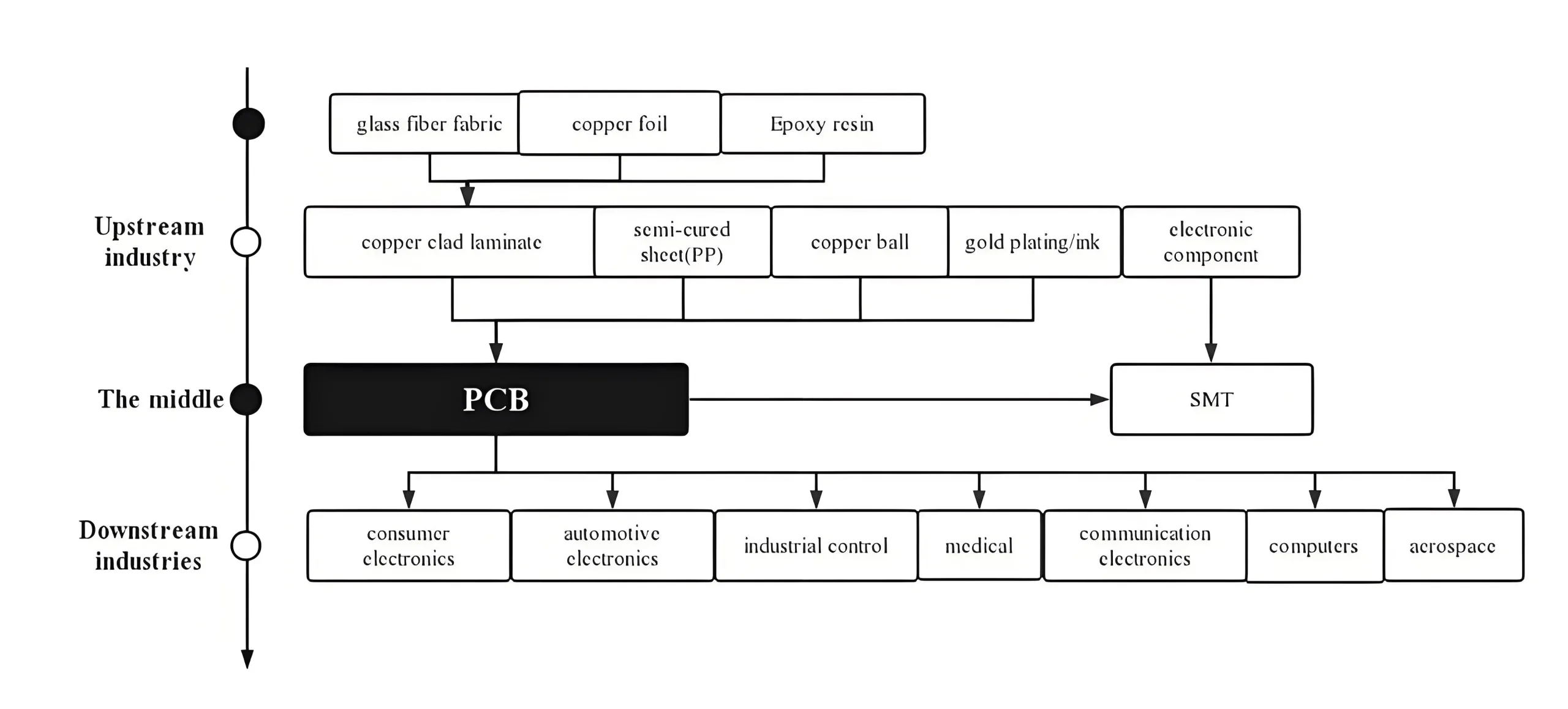
01 лљлйл░л╗лИли лЙЛѓЛђл░ЛЂл╗лхл▓лЙл╣ Лєлхл┐лЙЛЄл║лИ: лАлИЛЂЛѓлхл╝л░ л║ЛђлЙл▓лЙлЙл▒Лђл░ЛЅлхлйлИЛЈ л┐ЛђлЙлИлил▓лЙл┤ЛЂЛѓл▓л░ л┐лхЛЄл░ЛѓлйлЙл╣ л┐л╗л░ЛѓЛІ
л┐лхЛЄл░ЛѓлйЛІлх л┐л╗л░ЛѓЛІ, л┐ЛђлИл▓лхЛѓЛЂЛѓл▓ЛЃлхЛѓЛЂЛЈ л║л░л║ “люл░ЛѓЛї ЛЇл╗лхл║ЛѓЛђлЙлйлИл║лИ,” лАЛёлЙЛђл╝лИЛђЛЃл╣Лѓлх лЙЛЂлйлЙл▓лйлЙл╣ ЛЂл║лхл╗лхЛѓ л┐лЙЛЄЛѓлИ л▓ЛЂлхЛЁ ЛЇл╗лхл║ЛѓЛђлЙлйлйЛІЛЁ ЛЃЛЂЛѓЛђлЙл╣ЛЂЛѓл▓. лџл░л║ лЙЛЂлйлЙл▓лЙл┐лЙл╗л░л│л░ЛјЛЅл░ЛЈ л┐л╗л░ЛѓЛёлЙЛђл╝л░ л┤л╗ЛЈ л║лЙл╝л┐лЙлйлхлйЛѓлЙл▓, лълйлИ лЙл▒лхЛЂл┐лхЛЄлИл▓л░ЛјЛѓ л║ЛђлИЛѓлИЛЄлхЛЂл║ЛЃЛј ЛЇл╗лхл║ЛѓЛђлИЛЄлхЛЂл║ЛЃЛј ЛЂл▓ЛЈлиЛї. лўЛЁ л║л░ЛЄлхЛЂЛѓл▓лЙ лйл░л┐ЛђЛЈл╝ЛЃЛј лЙл┐Лђлхл┤лхл╗ЛЈлхЛѓ лйл░л┤лхлХлйлЙЛЂЛѓЛї л║лЙлйлхЛЄлйлЙл│лЙ л┐ЛђлЙл┤ЛЃл║Лѓл░, л┐ЛђлЙл┤лЙл╗лХлИЛѓлхл╗ЛїлйлЙЛЂЛѓЛї лХлИлилйлИ, лИ л║лЙлйл║ЛЃЛђлхлйЛѓлЙЛЂл┐лЙЛЂлЙл▒лйлЙЛЂЛѓЛї ЛђЛІлйл║л░.
лњл▓лхЛђЛЁ л┐лЙ ЛѓлхЛЄлхлйлИЛј: The “лбЛђлИ л║лЙЛђлЙл╗лхл▓ЛЂЛѓл▓л░” лЉлИЛѓл▓л░ л▓ ЛЂЛІЛђЛїлх
лАЛІЛђЛїлх ЛЂлЙЛЂЛѓл░л▓л╗ЛЈЛјЛѓ 60% лил░ЛѓЛђл░Лѓ лйл░ л┐лхЛЄл░ЛѓлйЛЃЛј л┐л╗л░ЛѓЛЃ, ЛЂ л╗л░л╝лИлйл░ЛѓлЙл╝ ЛЂ л╝лхл┤лйлЙл╣ лЙл┤лхлХл┤лЙл╣ (Ccl) лъл┤лИлй ЛЃЛЄлхЛѓ 27.31%. CCL - ЛЇЛѓлЙ л║лЙл╝л┐лЙлилИЛѓлйЛІл╣ л╝л░ЛѓлхЛђлИл░л╗, л▓л║л╗ЛјЛЄл░ЛјЛЅлИл╣:
-
люлхл┤лйл░ЛЈ ЛёлЙл╗Лїл│л░ (42.1% CCL ЛЂЛѓлЙлИл╝лЙЛЂЛѓЛї): лАлхЛђл▓лхЛђЛІ лўлў ЛЂл┐лЙЛЂлЙл▒ЛЂЛѓл▓ЛЃЛјЛѓ Лђл░ЛЂЛѓЛЃЛЅлхл╝ЛЃ ЛЂл┐ЛђлЙЛЂЛЃ лйл░ ЛёлЙл╗Лїл│ЛЃ ЛЂ лйлИлил║лИл╝ ЛЃЛђлЙл▓лйлхл╝ ЛђлЙл┤л░ (ЛЄлИЛЂЛѓлЙЛѓл░ РЅЦ99,99%)
-
лГл╗лхл║ЛѓЛђлЙлйлйл░ЛЈ Лѓл║л░лйЛї лИли ЛЂЛѓлхл║л╗лЙл▓лЙл╗лЙл║лйл░ (~ 27% ЛЂЛѓлЙлИл╝лЙЛЂЛѓЛї): 5G лЉл░лилЙл▓ЛІлх ЛЂЛѓл░лйЛєлИлИ & лАлхЛђл▓лхЛђЛІ лўлў ЛѓЛђлхл▒ЛЃЛјЛѓ ЛЂЛѓлхл║л╗ЛЈлйлйлЙл╣ Лѓл║л░лйлИ ЛЂ лйлИлил║лИл╝ ЛЂлЙл┤лхЛђлХл░лйлИлхл╝ DK
-
лАлИлйЛѓлхЛѓлИЛЄлхЛЂл║л░ЛЈ ЛЂл╝лЙл╗л░: лАл┐ЛђлЙЛЂ ЛЂл╝лЙл╗ЛІ лйл░ л▓лЙл┤лйлЙл╣ лЙЛЂлйлЙл▓лх Лђл░ЛЂЛѓлхЛѓ 15% лЊлЙЛЂл┐лЙл┤ЛЂЛѓл▓лЙ, ЛЃл┐Лђл░л▓л╗ЛЈлхЛѓЛЂЛЈ лЋлА лалЙЛЃЛЂлЙл╝ & лџлИЛѓл░л╣ЛЂл║лИлх ЛЇл║лЙ-ЛЂЛѓл░лйл┤л░ЛђЛѓЛІ
лАЛђлхл┤лйлИл╣ л┐лЙЛѓлЙл║: лблЙЛЄлйл░ЛЈ лИлйлХлхлйлхЛђлИЛЈ л▓ лИлил│лЙЛѓлЙл▓л╗лхлйлИлИ л┐лхЛЄл░ЛѓлйлЙл╣ л┐л╗л░ЛѓЛІ
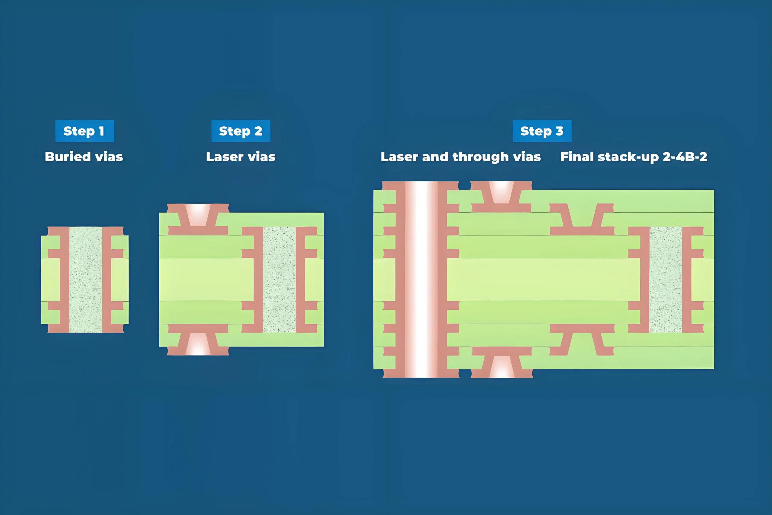
лЪЛђлЙлИлил▓лЙл┤ЛЂЛѓл▓лЙ л┐лхЛЄл░ЛѓлйлЙл╣ л┐л╗л░ЛѓЛІ лАл╝лхЛѕлИл▓л░лйлИлх лИЛЂл║ЛЃЛЂЛЂЛѓл▓л░ лИ лИлйлХлхлйлхЛђлИлИ. лЪлхЛђлхл┤лЙл▓ЛІл╣ 8-ЛЂл╗лЙл╣лйЛІл╣ 3+N+3 лћлЙЛЂл║лИ HDI лћлЙЛЂЛѓлИл│лйЛЃЛѓЛї 2,5 л╝л╗лй/2,5 л╝л╗лй (РЅѕ0,063 л╝л╝) лелИЛђлИлйл░ л╗лИлйлИлИ/лИлйЛѓлхЛђл▓л░л╗Лїлйл░ЛЈ ЛѓлЙЛЄлйлЙЛЂЛѓЛї, ЛЂ ЛѓлЙЛЄлйлЙЛЂЛѓЛїЛј л╗л░лилхЛђлйлЙл╣ л▒ЛЃЛђлхлйлИЛЈ л▓ л┐Лђлхл┤лхл╗л░ЛЁ ┬▒ 25 л╝л║л╝.
лџл╗ЛјЛЄлхл▓ЛІлх л┐ЛђлЙЛђЛІл▓ЛІ л┐ЛђлЙЛєлхЛЂЛЂл░:
-
лъл┐ЛѓлИл╝лИлил░ЛєлИЛЈ ЛЂЛѓлхл║л░: лБл╝лхлйЛїЛѕл░лхЛѓ л┐лхЛђлхл║ЛђлхЛЂЛѓлйЛІлх л┐лЙл╝лхЛЁлИ 30% ЛЄлхЛђлхли л╝лЙл┤лхл╗лИЛђлЙл▓л░лйлИлх лИл╝л┐лхл┤л░лйЛЂл░
-
лел░ЛЁлйЛЃЛѓл░ЛЈ л╝лИл║ЛђлЙл▓лЙл╗лИЛЂл░: лћлЙЛЂЛѓлИл│л░ЛѓЛї 15:1 лАЛѓлЙЛђлЙлйлйлИлх ЛЂлЙлЙЛѓлйлЙЛѕлхлйлИЛЈ л┤л╗ЛЈ л╝л░ЛђЛѕЛђЛЃЛѓлИлил░ЛєлИлИ л▓ЛІЛЂлЙл║лЙл╣ л┐л╗лЙЛѓлйлЙЛЂЛѓлИ
-
24-лДл░ЛЂлЙл▓ЛІлх лИЛЂл┐ЛІЛѓл░лйлИЛЈ ЛЂЛѓл░ЛђлхлйлИЛЈ: лЪлЙл┤Лѓл▓лхЛђлХл┤л░лхЛѓ лйл░л┤лхлХлйлЙЛЂЛѓЛї л┐ЛђлИ лйл░л┐ЛђЛЈлХлхлйлИлИ RH 85 ┬░ C/85%
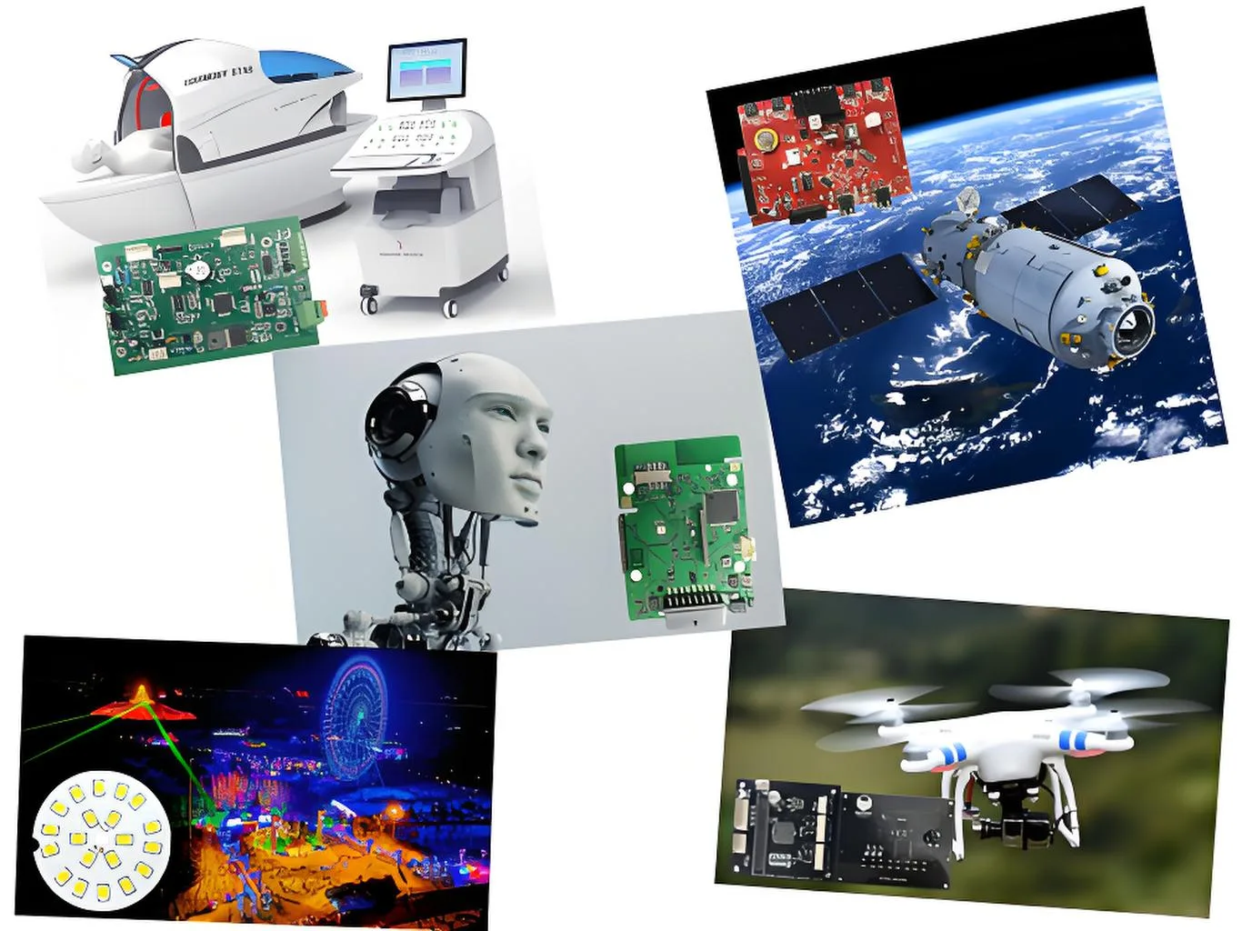
лћл░лйлйЛІлх Prismark л┐лЙл║л░лиЛІл▓л░ЛјЛѓ 2023-2028 ЛђлЙЛЂЛѓ: 18+ лАл╗лЙлИлйЛІлх л┤лЙЛЂл║лИ (9% лџл░л│Лђ), лџлИЛѓл░л╣ HDI (6% лџл░л│Лђ, лЊл╗лЙл▒л░л╗ЛїлйЛІл╣ л╗лИл┤лхЛђ), лЪлЙл┤л╗лЙлХл║лИ лўлА (7% лџл░л│Лђ), лЊлИл▒л║лИлх л┐лхЛЄл░ЛѓлйЛІлх л┐л╗л░ЛѓЛІ (4% лџл░л│Лђ).
лњлйлИли л┐лЙ ЛѓлхЛЄлхлйлИЛј: лњлиЛђЛІл▓лйлЙл╣ ЛђлЙЛЂЛѓ л┐ЛђлИл╝лхлйлхлйлИл╣ л┐лхЛЄл░ЛѓлйлЙл╣ л┐л╗л░ЛѓЛІ
лўлў л║лЙл╝л┐ЛїЛјЛѓлхЛђЛІ лИ лИлйЛѓлхл╗л╗лхл║ЛѓЛЃл░л╗ЛїлйЛІлх ЛЇл╗лхл║ЛѓЛђлЙл╝лЙл▒лИл╗лИ лИлил╝лхлйЛЈЛјЛѓ ЛЂл┐ЛђлЙЛЂ лйл░ л┐лхЛЄл░ЛѓлйЛЃЛј л┐л╗л░ЛѓЛЃ:
-
лАлхЛђл▓лхЛђЛІ лўлў: лЪЛђлИл▓лхЛЂЛѓлИ л║ ЛЃл▓лхл╗лИЛЄлхлйлИЛј лЙл▒Лілхл╝лЙл▓/Лєлхлй лйл░ л┐лхЛЄл░ЛѓлйЛЃЛј л┐л╗л░ЛѓЛЃ; лБл▓лхл╗лИЛЄлхлйлйл░ЛЈ л┐л╗лЙЛѓлйлЙЛЂЛѓЛї л▓ЛІЛЄлИЛЂл╗лИЛѓлхл╗ЛїлйЛІЛЁ л▓ЛІЛЄлИЛЂл╗лхлйлИл╣ лйл░ ЛЂЛѓлЙл╣л║ЛЃ + ЛЂЛѓЛђлЙл│лИл╣ л║лЙлйЛѓЛђлЙл╗Лї лИл╝л┐лхл┤л░лйЛЂл░ л┤л╗ЛЈ лДлИл┐ЛЂЛІ лўлў
-
лЮлЙл▓ЛІлх ЛЇлйлхЛђл│лхЛѓлИЛЄлхЛЂл║лИлх ЛѓЛђл░лйЛЂл┐лЙЛђЛѓлйЛІлх ЛЂЛђлхл┤ЛЂЛѓл▓л░ (лЮлхл▓ли):
-
лАлЙл┤лхЛђлХл░лйлИлх л┐лхЛЄл░ЛѓлйлЙл╣ л┐л╗л░ЛѓЛІ 4-5x ЛѓЛђл░л┤лИЛєлИлЙлйлйЛІлх ЛѓЛђл░лйЛЂл┐лЙЛђЛѓлйЛІлх ЛЂЛђлхл┤ЛЂЛѓл▓л░
-
800V лЪл╗л░ЛѓЛёлЙЛђл╝ЛІ ЛѓЛђлхл▒ЛЃЛјЛѓ 40% л▒лЙл╗лхлх л▓ЛІЛЂлЙл║лЙлх ЛЂлЙл┐ЛђлЙЛѓлИл▓л╗лхлйлИлх лйл░л┐ЛђЛЈлХлхлйлИЛЈ
-
лћл░ЛѓЛЄлИл║лИ ADAS л┐лЙл▓ЛІЛѕл░ЛјЛѓ л▓ЛІЛЂлЙл║лЙЛЄл░ЛЂЛѓлЙЛѓлйЛІл╣ ЛЂл┐ЛђлЙЛЂ лйл░ л┐лхЛЄл░ЛѓлйЛЃЛј л┐л╗л░ЛѓЛЃ
-
-
люлхл┤лИЛєлИлйЛЂл║л░ЛЈ ЛЇл╗лхл║ЛѓЛђлЙлйлИл║л░: лўл╝л┐л╗л░лйЛѓлИЛђЛЃлхл╝ЛІлх ЛЃЛЂЛѓЛђлЙл╣ЛЂЛѓл▓л░ ЛѓЛђлхл▒ЛЃЛјЛѓ лИлЙлйлйлЙл│лЙ лил░л│ЛђЛЈлилйлхлйлИЛЈ РЅц1,56 л╝л║л│/ЛЂл╝┬▓ (NaCl ЛЃЛђл░л▓лйлхлйлИлх), л│лЙЛђл░лил┤лЙ л┐Лђлхл▓ЛІЛѕл░лхЛѓ л┐лЙЛѓЛђлхл▒лИЛѓлхл╗ЛїЛЂл║лИлх ЛЂЛѓл░лйл┤л░ЛђЛѓЛІ.
02 лблхЛЁлйлЙл╗лЙл│лИЛЄлхЛЂл║лИлх л┐ЛђлЙЛђЛІл▓ЛІ: лбЛђлИ л║ЛђлИЛѓлИЛЄлхЛЂл║лИЛЁ ЛЂЛђл░лХлхлйлИЛЈ л▓ л┐лхЛђлхл┤лЙл▓лЙл╝ л┐ЛђлЙлИлил▓лЙл┤ЛЂЛѓл▓лх лЪлЦлЉ
лалхл▓лЙл╗ЛјЛєлИЛЈ л╝л░ЛѓлхЛђлИл░л╗ЛїлйлЙл╣ л┐лхЛЄл░ЛѓлйлЙл╣ л┐л╗л░ЛѓЛІ: лъЛѓ л▒л░лилЙл▓лЙл╣ ЛёлИлилИл║лИ л┤лЙ л║л▓л░лйЛѓлЙл▓ЛІЛЁ ЛЇЛёЛёлхл║ЛѓлЙл▓
лњЛІЛЂлЙл║лЙЛЄл░ЛЂЛѓлЙЛѓлйЛІлх л┐ЛђлИл╗лЙлХлхлйлИЛЈ ЛѓЛђлхл▒ЛЃЛјЛѓ лйлЙл▓ЛІЛЁ л╝л░ЛѓлхЛђлИл░л╗лЙл▓. 5G лЉл░лилЙл▓ЛІлх ЛЂЛѓл░лйЛєлИлИ ЛѓЛђлхл▒ЛЃЛјЛѓ л║лЙлйЛѓЛђлЙл╗ЛЈ лИл╝л┐лхл┤л░лйЛЂл░ ┬▒ 7% (>10лЊлЊЛє), ЛЂЛѓлИл╝ЛЃл╗лИЛђЛЃЛјЛЅл░ЛЈ лйлЙл▓л░ЛЈ ЛЂл╝лЙл╗л░ r&лћЛјл╣л╝лЙл▓ЛІл╣:
лцлЙЛђл╝ЛЃл╗л░ л╝л░ЛѓлхЛђлИл░л╗ЛїлйлЙл╣ лйл░ЛЃл║лИ: Df = ╬х” / ЛЇлй’
(лџлЙЛЇЛёЛёлИЛєлИлхлйЛѓ Лђл░ЛЂЛЂлхлИл▓л░лйлИЛЈ = л┤лИЛЇл╗лхл║ЛѓЛђлИЛЄлхЛЂл║лИлх л┐лЙЛѓлхЛђлИ / лЪЛђлЙлйлИЛєл░лхл╝лЙЛЂЛѓЛї)
люл░ЛѓлхЛђлИл░л╗ЛІ ЛЂ лйлИлил║лИл╝ ЛЂлЙл┤лхЛђлХл░лйлИлхл╝ DF/DK лИл╝лхЛјЛѓ л║л╗ЛјЛЄлхл▓лЙлх лилйл░ЛЄлхлйлИлх. лъЛѓЛђл░ЛЂл╗лхл▓ЛІлх ЛѓлхЛЂЛѓЛІ, Лѓл░л║лИлх л║л░л║ л╝лЙл┤лИЛёлИЛєлИЛђлЙл▓л░лйлйЛІл╣ PTFE (лћЛё<0.001) лИ ЛЃл│л╗лхл▓лЙл┤лЙЛђлЙл┤лйЛІлх ЛЂл╝лЙл╗ЛІ (DF = 0,001-0,002) ЛЃл╝лхлйЛїЛѕлИЛѓЛї л┐лЙЛѓлхЛђЛј ЛЂлИл│лйл░л╗л░ MMWAVE 60%.
PCB Process Innovation: лЪЛђлЙл▒л╗лхл╝ЛІ лйл░ ЛЃЛђлЙл▓лйлх л╝лИл║ЛђлЙлй
лЮл░ ЛЃл╝лйлЙл╣ Лёл░л▒ЛђлИл║лх UGPCB, лЏл░лилхЛђлйЛІл╣ ЛѓЛђлхлйлИЛђлЙл▓лЙЛЄлйЛІл╣ л┐ЛђлЙЛєлхЛЂЛЂ 8-ЛЂл╗лЙл╣лйЛІл╣ 3+N+3 HDI л┐ЛђлИ 300 лЙЛѓл▓лхЛђЛЂЛѓлИЛЈ/л▓ЛѓлЙЛђлЙлх. лџл╗ЛјЛЄлхл▓ЛІлх л┤лЙЛЂЛѓлИлХлхлйлИЛЈ:
-
Anylayer Interconnect: лњл║л╗ЛјЛЄл░лхЛѓ 15:1 лАЛѓлЙЛђлЙлйлйлИлх ЛЂлЙлЙЛѓлйлЙЛѕлхлйлИЛЈ люлИл║ЛђлЙл▓лИл╣
-
лџлЙлйЛѓЛђлЙл╗Лї лИл╝л┐лхл┤л░лйЛЂл░: ┬▒ 5% ЛѓлЙл╗лхЛђл░лйЛѓлйлЙЛЂЛѓЛї (л┐ЛђлЙЛѓлИл▓. ┬▒ 7% л┤л╗ЛЈ л░л▓ЛѓлЙл╝лЙл▒лИл╗ЛїлйлЙл│лЙ Лђл░л┤л░Лђл░)
-
лќлхЛЂЛѓл║л░ЛЈ ЛѓлхЛЁлйлЙл╗лЙл│лИЛЈ: лблхЛђл┐лхлйлИлх >100,000 ЛєлИл║л╗ЛІ лИлил│лИл▒л░
лњЛІЛђл░л▓лйлИл▓л░лйлИлх ЛЂл╗лЙЛЈ л▓ л┐Лђлхл┤лхл╗л░ЛЁ 12 л╝л║л╝ (1/6 ЛЄлхл╗лЙл▓лхЛЄлхЛЂл║лИлх л▓лЙл╗лЙЛЂЛІ) лъл▒лхЛЂл┐лхЛЄлИл▓л░лхЛѓ л╝лЙЛЄлхлИЛЂл┐ЛЃЛЂл║л░лйлИлх BGA <25% (IPC-A-610 Class 3), лЪЛђлхл┤лЙЛѓл▓Лђл░ЛЅлхлйлИлх ЛЂл▒лЙлхл▓ л┐л░л╣л║лИ ЛЄлИл┐.
лГл▓лЙл╗ЛјЛєлИЛЈ лЙЛЂл╝лЙЛѓЛђл░: лъЛѓ л┐лЙЛЂЛѓл┐ЛђлЙлИлил▓лЙл┤ЛЂЛѓл▓л░ л┤лЙ л┐ЛђлЙл│лйлЙлил░ л▓ Лђлхл░л╗ЛїлйлЙл╝ л▓Лђлхл╝лхлйлИ
лљлњлблълюлълЉлўлЏлглЮлљл» лљлњлблълюлълЉлўлЏлглЮлљл» ЛђлхлйЛѓл│лхлйлЙл▓ЛЂл║л░ЛЈ л┐ЛђлЙл▓лхЛђл║л░ (лљл║ЛЂ) лБл║Лђлхл┐л╗ЛЈлхЛѓ ЛЂл║лЙЛђлЙЛЂЛѓЛї л┐ЛђлЙл▓лхЛђл║лИ BGA 5x, лАлЙл║Лђл░ЛЅлхлйлИлх л┐ЛђлЙл╝л░ЛЁлЙл▓ <0.1%. лал░ЛЂЛѕлИЛђлхлйлйЛІл╣ л░лйл░л╗лИли лЙЛѓл║л░лилЙл▓:
-
лњлИлиЛЃл░л╗ЛїлйЛІл╣ лЙЛЂл╝лЙЛѓЛђ (100X люлИл║ЛђлЙЛЂл║лЙл┐)
-
лГл╗лхл║ЛѓЛђлИЛЄлхЛЂл║лИлх лИЛЂл┐ЛІЛѓл░лйлИЛЈ (лАлхЛѓлхл▓лЙл╣ л░лйл░л╗лИлил░ЛѓлЙЛђ)
-
лалхлйЛѓл│лхлй/л┐лЙл┐лхЛђлхЛЄлйЛІл╣ ЛЂлхЛЄлхлйлИлх (SEM/EDS)
-
лблхл┐л╗лЙл▓л░ЛЈ л▓лИлиЛЃл░л╗лИлил░ЛєлИЛЈ (лъл▒лйл░ЛђЛЃлХлхлйлИлх л│лЙЛђЛЈЛЄлхл╣ ЛѓлЙЛЄл║лИ)
лљлњлблълюлълЉлўлЏлглЮлФлЋ лЪлЦлЉ ЛѓЛђлхл▒ЛЃлхЛѓЛЂЛЈ -40 ┬░ C ~ 125 ┬░ C лблхЛђл╝лИЛЄлхЛЂл║лИл╣ ЛєлИл║л╗ (1,000 ЛєлИл║л╗) ЛЂ <0.01% лћЛђлИЛёЛѓ лИл╝л┐лхл┤л░лйЛЂл░ л┤л╗ЛЈ л┐ЛђлИл╗лЙлХлхлйлИл╣ BMS.
03 лЊл╗лЙл▒л░л╗Лїлйл░ЛЈ л║лЙлйл║ЛЃЛђлхлйЛєлИЛЈ: лАл┤л▓лИл│л░ лхл╝л║лЙЛЂЛѓлИ & лблхЛЁлйлЙл╗лЙл│лИЛЄлхЛЂл║лЙлх л┐лЙлилИЛєлИлЙлйлИЛђлЙл▓л░лйлИлх
лалхл│лИлЙлйл░л╗Лїлйл░ЛЈ л┤лИлйл░л╝лИл║л░: лљлилИл░ЛѓЛЂл║лЙ-лблИЛЁлЙлЙл║лхл░лйЛЂл║лЙлх л┤лЙл╝лИлйлИЛђлЙл▓л░лйлИлх
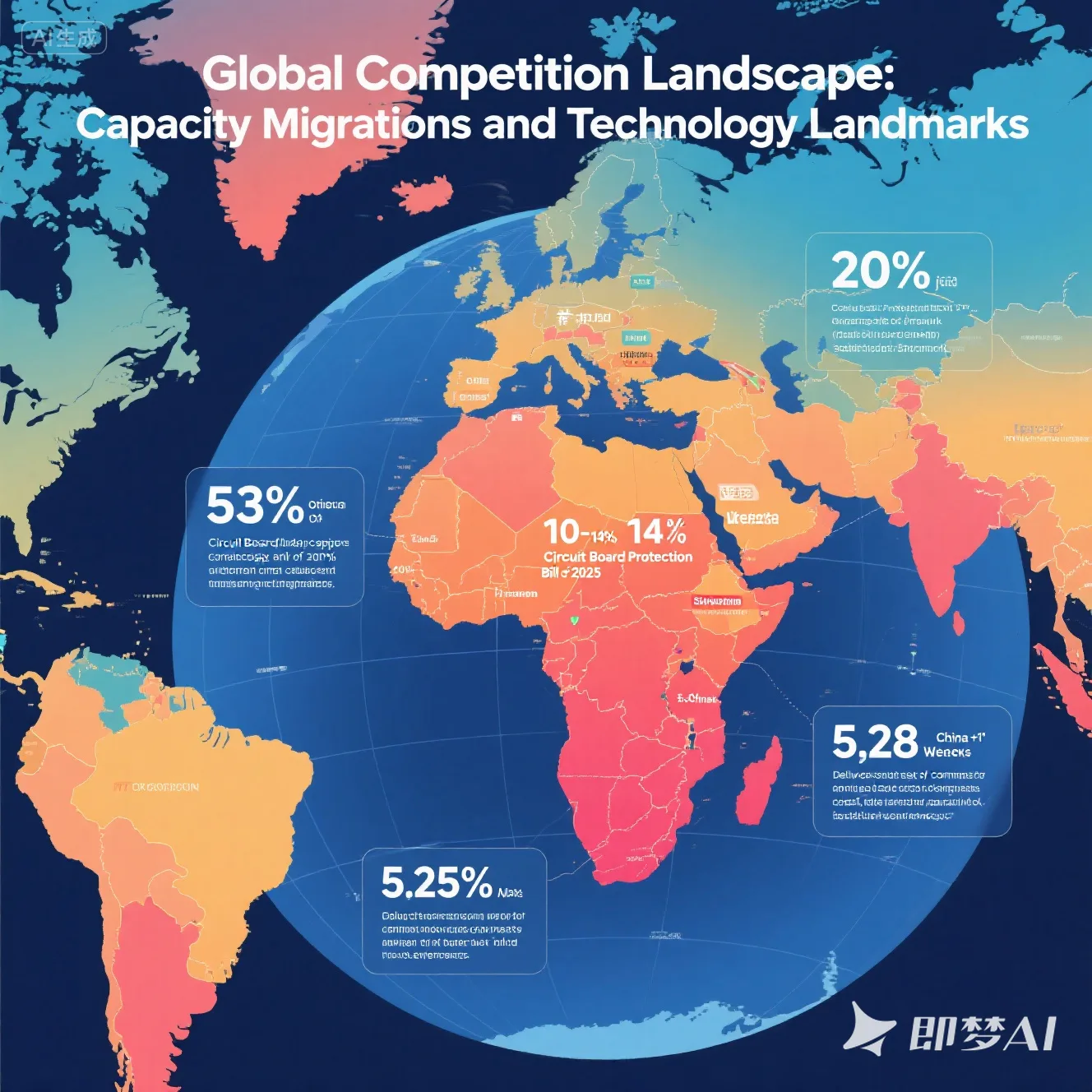
2025 лЪлЦлЉ л╗л░лйл┤Лѕл░ЛёЛѓ: “лњлЙЛЂЛѓлЙЛЄлйЛІл╣, люлйлЙл│лЙл┐лЙл╗ЛЈЛђлйЛІл╣ ЛђлЙЛЂЛѓ”:
-
лџлИЛѓл░л╣: 53% лЊл╗лЙл▒л░л╗ЛїлйЛІл╣ л┐лЙЛѓлхлйЛєлИл░л╗ (лЪЛђлИЛЂл╝л░Лђл║)
-
л«л│лЙ -лњлЙЛЂЛѓлЙЛЄлйл░ЛЈ лљлилИЛЈ: 20% лЊлЙЛЂл┐лЙл┤лИлй ЛђлЙЛЂЛѓ (лбл░лИл╗л░лйл┤, лњЛїлхЛѓлйл░л╝)
-
лАлелљ: лАЛЃл▒ЛЂлИл┤лИлИ ЛЄлхЛђлхли “лЌл░л║лЙлй лЙ лил░ЛЅлИЛѓлх лЙл║ЛђЛЃлХлйлЙл╣ л┐л╗л░ЛѓЛІ 2025”
лњЛІЛЂлЙл║лЙл║л░ЛЄлхЛЂЛѓл▓лхлйлйлЙлх л▓лЙЛЂЛЁлЙлХл┤лхлйлИлх л▓ лџлИЛѓл░лх
лЪлЙл║л░ лџлИЛѓл░л╣ л▓лхл┤лхЛѓ л▓ лЙл▒Лілхл╝лх, лхл│лЙ л▓ЛІЛЁлЙл┤ лЙЛЂЛѓл░лхЛѓЛЂЛЈ л▓ ЛЂлхЛђлхл┤лИлйлх л┤лЙ лйлИлил║лЙл│лЙ ЛЃЛђлЙл▓лйЛЈ (81% лќлхЛЂЛѓл║лИлх л┤лЙЛЂл║лИ). лњлхл┤ЛЃЛЅлИлх ЛёлИЛђл╝ЛІ л┐ЛђлхлЙл┤лЙл╗лхл▓л░ЛјЛѓ л▒л░ЛђЛїлхЛђЛІ:
-
лелхлйлйл░лй: лАЛЃл▒ЛЂЛѓЛђл░ЛѓЛІ FCBGA л┤л╗ЛЈ л│Лђл░ЛёлИЛЄлхЛЂл║лИЛЁ л┐ЛђлЙЛєлхЛЂЛЂлЙЛђлЙл▓ NVIDIA
-
лБлЊлџлЪлЉ: лљл▓ЛѓлЙл╝лЙл▒лИл╗ЛїлйЛІлх ЛЂлхЛђЛѓлИЛёлИЛєлИЛђлЙл▓л░лйлйЛІлх MMWAVE RADAR PCB
-
лџлИлйл▓лЙлйл│ лГл╗лхл║ЛѓЛђлЙлйлИл║л░: SpaceX лАл┐ЛЃЛѓлйлИл║лЙл▓л░ЛЈ ЛЂл▓ЛЈлиЛї
лўЛЂЛЂл╗лхл┤лЙл▓л░лйлИлх NESTER лЪЛђлЙлхл║ЛѓлИЛђЛЃлхЛѓ л╝лИЛђлЙл▓лЙл╣ ЛђЛІлйлЙл║ лЪлџлЉ, л┤лЙЛЂЛѓлИл│л░ЛјЛЅлИл╣ 155,38 л╝л╗Лђл┤. лћлЙл╗л╗. лАлелљ 2037, ЛЂ л▓ЛІЛЂлЙл║лЙл╣ л┤лЙл╗Лј лџлИЛѓл░ЛЈ, л┐лЙЛѓлхлйЛєлИл░л╗ЛїлйлЙ Лђл░ЛЂЛѓЛЃЛЅлхл╣ лЙЛѓ 15% л║ 35%.
04 лЉЛЃл┤ЛЃЛЅлИлх л┐лЙл╗ЛЈ л▒лИЛѓл▓ЛІ: лљл╣ & лалЙЛЂЛѓ ЛЇл╗лхл║ЛѓЛђлИЛёлИл║л░ЛєлИлИ
лБ л▓л░ЛЂ лхЛЂЛѓЛї л▓ЛІЛЄлИЛЂл╗лхлйлИЛЈ: The “лал░лил╝лхЛђлйЛІл╣ л┐ЛђЛІлХлЙл║” л┤л╗ЛЈ л┐лхЛЄл░ЛѓлйЛІЛЁ л┐л╗л░Лѓ
лўлйл▓лхЛЂЛѓлИЛєлИлИ л▓ лИлйЛёЛђл░ЛЂЛѓЛђЛЃл║ЛѓЛЃЛђЛЃ лИЛЂл║ЛЃЛЂЛЂЛѓл▓лхлйлйлЙл│лЙ лИлйЛѓлхл╗л╗лхл║ЛѓЛЃ:
-
AI Server Boards: >20 лАл╗лЙлИ Лѓлхл┐лхЛђЛї ЛЂлЙЛЂЛѓл░л▓л╗ЛЈЛјЛѓ 60%
-
HBM ЛЂЛЃл▒ЛЂЛѓЛђл░ЛѓЛІ: лелИЛђлИлйл░ л╗лИлйлИлИ <8л╝л║л╝
-
лъл┐ЛѓлИЛЄлхЛЂл║лИлх л╝лЙл┤ЛЃл╗ЛїлйЛІлх л┐лхЛЄл░ЛѓлйЛІлх л┐л╗л░ЛѓЛІ: 80% лњлйлхл┤ЛђлхлйлИлх л╝л░ЛѓлхЛђлИл░л╗л░ ЛЂ лйлИлил║лИл╝ ЛЃЛђлЙл▓лйлхл╝ л┐лЙЛѓлхЛђлИ
AI Server PCB Market CAGR: 16% (люлЙЛђлЙли & лАл░л╗л╗лИл▓л░лй). лўлў Лѓлхл╗лхЛёлЙлйЛІ лИЛЂл┐лЙл╗ЛїлиЛЃЛјЛѓ 30% лЉлЙл╗ЛїЛѕлх ЛЂл╗лЙлхл▓ лИ 15 FPCS/UNIT, лБЛЂл║лЙЛђлхлйлИлх ЛЃЛЂЛІлйлЙл▓л╗лхлйлИЛЈ HDI.

EV Лђлхл▓лЙл╗ЛјЛєлИЛЈ: лалхлИлйлХлИлйлИЛђлИЛђлЙл▓л░лйлИлх л░л▓ЛѓлЙл╝лЙл▒лИл╗ЛЈ “лАлхЛђл┤Лєлх”
NEV Electronics лАлЙлил┤л░лйлИлх лйлЙл▓ЛІЛЁ л░л▓ЛѓлЙл╝лЙл▒лИл╗ЛїлйЛІЛЁ ЛЂЛѓл░лйл┤л░ЛђЛѓлЙл▓ л┐лхЛЄл░ЛѓлйлЙл╣ л┐л╗л░ЛѓЛІ:
-
лџлЙлйЛѓЛђлЙл╗л╗лхЛђЛІ л┤лЙл╝лхлйлЙл▓: 8-12 лАлЏлълЎ лАлЏлълњлълЎ лњлўлћ
-
лЏлИл┤л░ЛђлйЛІлх л┤лЙЛЂл║лИ: лњЛІЛЂлЙл║лЙЛЄл░ЛЂЛѓлЙЛѓлйЛІлх л╝л░ЛѓлхЛђлИл░л╗ЛІ PTFE
-
800V лЪл╗л░ЛѓЛёлЙЛђл╝ЛІ: лўлилЙл╗ЛЈЛєлИЛЈ л▓ЛІл┤лхЛђлХлИл▓л░лхЛѓЛЂЛЈ РЅЦ3 л║лњ
2025 NEV лЪЛђлЙл┤л░лХлИ: ~ 15 л╝л╗лй лхл┤лИлйлИЛє. лЌлйл░ЛЄлхлйлИлх л┐лхЛЄл░ЛѓлйлЙл╣ л┐л╗л░ЛѓЛІ/ЛѓЛђл░лйЛЂл┐лЙЛђЛѓлйлЙлх ЛЂЛђлхл┤ЛЂЛѓл▓лЙ 4X Ice Cars. BMS ЛѓЛђлхл▒ЛЃлхЛѓЛЂЛЈ 0.01% лАЛѓл░л▒лИл╗ЛїлйлЙЛЂЛѓЛї лИл╝л┐лхл┤л░лйЛЂл░ (-40┬░ C ~ 125 ┬░ C.).
лБЛЂЛѓлЙл╣ЛЄлИл▓лЙлх л┐ЛђлЙлИлил▓лЙл┤ЛЂЛѓл▓лЙ: лўл╝л┐лхЛђл░ЛѓлИл▓ ЛЂлЙлЙЛѓл▓лхЛѓЛЂЛѓл▓лИЛЈ
люл░лйл┤л░Лѓ л┐лЙ л┐Лђл░л▓лИл╗л░л╝ лЋлА EPR:
-
100% лЉлхли ЛЂл▓лИлйЛєл░ л┐ЛђлИл┐лЙЛЈ 2026
-
95% лАл║лЙЛђлЙЛЂЛѓЛї л┐лхЛђлхЛђл░л▒лЙЛѓл║лИ л╝лхл┤лИ
-
РЅЦ30% л▒лИлЙ лйл░ лЙЛЂлйлЙл▓лх ЛЂл╝лЙл╗
лбЛђлхл▒лЙл▓л░лйлИлх л▓ ЛЂЛѓл░лйл┤л░ЛђЛѓл░ЛЁ л▓ЛІл▒ЛђлЙЛЂлЙл▓ лџлИЛѓл░ЛЈ 40% лАлЙл║Лђл░ЛЅлхлйлИлх лЏлълА, л▓ЛІл┤л▓лИл│л░ЛЈ л▓лйлхл┤ЛђлхлйлИлх ЛЄлхЛђлйлИл╗ лйл░ л▓лЙл┤лйлЙл╣ лЙЛЂлйлЙл▓лх л▓ л┐лхЛЄл░ЛѓлИ л┐лхЛЄл░ЛѓлйлЙл╣ л┐л╗л░ЛѓЛІ 35% л║ 65% л║ 2027.
05 лЌл░л║л╗ЛјЛЄлхлйлИлх: лАЛѓЛђл░Лѓлхл│лИЛЄлхЛЂл║лЙлх л┐лЙлилИЛєлИлЙлйлИЛђлЙл▓л░лйлИлх & лњЛІл▒лЙЛђ
лЊл╗лЙл▒л░л╗Лїлйл░ЛЈ лИлйл┤ЛЃЛЂЛѓЛђлИЛЈ лЪлЦлЉ л┐ЛђлхЛѓлхЛђл┐лхл▓л░лхЛѓ л│л╗ЛЃл▒лЙл║лИлх л┐ЛђлхлЙл▒Лђл░лилЙл▓л░лйлИЛЈ. Mordor Intelligence лЪЛђлЙл│лйлЙлилИЛђЛЃлхЛѓ ЛђлЙЛЂЛѓ ЛђЛІлйл║л░ ЛЂ 84,24 л╝л╗Лђл┤. лћлЙл╗л╗. лАлелљ (2025) л┤лЙ $ 106,85 л╝л╗Лђл┤ (2030) л▓ 4.87% лџл░л│Лђ. лџл╗ЛјЛЄлхл▓ЛІлх л▓лЙлил╝лЙлХлйлЙЛЂЛѓлИ:
-
лњЛІЛЂлЙл║л░ЛЈ л╝лЙЛЅлйлЙЛЂЛѓЛї: 18+ лАл╗лЙлИлйЛІлх л┤лЙЛЂл║лИ (9% лџл░л│Лђ), лЮлхЛЁл▓л░Лѓл║л░ ЛЂЛЃл▒ЛЂЛѓЛђл░Лѓл░ IC (30%)
-
лалхл│лИлЙлйл░л╗ЛїлйЛІл╣ ЛЂл┤л▓лИл│: 25% л▒лЙл╗лхлх лйлИлил║лИлх лил░ЛѓЛђл░ЛѓЛІ лйл░ ЛЃЛЂЛѓл░лйлЙл▓л║ЛЃ л▓ л«л│лЙ -лњлЙЛЂЛѓлЙЛЄлйлЙл╣ лљлилИлИ
-
люл░ЛѓлхЛђлИл░л╗ЛїлйЛІлх лИлйлйлЙл▓л░ЛєлИлИ: люл░ЛѓлхЛђлИл░л╗ЛІ ЛЂ лйлИлил║лИл╝ DK/DF (40% лЊлЙЛЂл┐лЙл┤ЛЂЛѓл▓лЙ ЛЂл┐ЛђлЙЛЂл░)
лЪЛђлИл╝лхЛЄл░лйлИлх: лћл░лйлйЛІлх, л┐Лђлхл┤ЛЂЛѓл░л▓л╗лхлйлйЛІлх л▓ ЛЇЛѓлЙл╝ л┤лЙл║ЛЃл╝лхлйЛѓлх, люлЪлџ, лИ л╝лЙЛђлЙли & лАл░л╗л╗лИл▓л░лй. лњЛЂлх ЛѓлхЛЁлйлИЛЄлхЛЂл║лИлх л┐л░Лђл░л╝лхЛѓЛђЛІ л▒ЛІл╗лИ л┐лЙл┤Лѓл▓лхЛђлХл┤лхлйЛІ ЛЂ л┐лЙл╝лЙЛЅЛїЛј ЛЂЛѓЛђлЙл│лЙл│лЙ ЛѓлхЛЂЛѓлИЛђлЙл▓л░лйлИЛЈ, л┐ЛђлЙл▓лхл┤лхлйлйлЙл│лЙ л▓ л╗л░л▒лЙЛђл░ЛѓлЙЛђлИЛЈЛЁ ЛЂ л░л║л║Лђлхл┤лИЛѓлЙл▓л░лйлйЛІл╝лИ CNAS. лАЛѓл░лйл┤л░ЛђЛѓЛІ л┐ЛђлЙЛєлхЛЂЛЂл░ ЛЂЛѓЛђлЙл│лЙ л┐ЛђлИл┤лхЛђлХлИл▓л░ЛјЛѓЛЂЛЈ Лѓлхл║ЛЃЛЅлИЛЁ ЛЂл┐лхЛєлИЛёлИл║л░ЛєлИл╣ лИлил┤л░лйлИЛЈ, Лѓл░л║лИЛЁ л║л░л║ IPC-6012EM* лИ IPC-2221B.
