

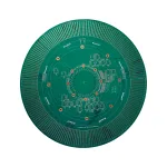
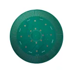
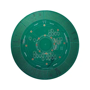
Введение в печатную плату с картой зонда UGPCB
50-х слоя UGPCB съел (Автоматизированное испытательное оборудование) Зонд карта печатная плата является точным инженерным раствором, предназначенным для высокочастотных полупроводниковых испытаний. Это обеспечивает точную передачу сигнала между тестовым оборудованием и интегрированными цепями (ICS), Обеспечение надежной производительности в критически важной среде.
Ключевые технические характеристики
-
Количество слоев: 50 слои
-
Толщина: 198 мил
-
Материал: FR4 Htg (Высокотемпературная стеклянная эпоксидная смола)
-
Минимальный размер отверстия: 5 мил
-
BGA -интервал: 0.35мм
- Толщина меди:2/2унция
-
Соотношение сторон: 40:1
-
Расстояние для тренировки: 3 мил
-
Пофв (Нанесенный наполненным через): Да
-
Поверхностная отделка: Энэг (Электролетное никелевое электролетное золото)
Дизайн и структурные инновации
Критические особенности дизайна
-
Взаимодействие высокой плотности: 50-слойная архитектура поддерживает ультралепую маршрутизацию для компонентов BGA с высоте 0,35 мм, необходимо для современного тестирования IC.
-
Продвинутый материал: FR4 HTG обеспечивает тепловую стабильность (TG ≥ 180 ° C), Предотвращение деформации во время мощных циклов тестирования.
-
Точное бурение: А 40:1 Соотношение сторон и 5 MIL Microvias включает надежные пути сигнала в плотно расположенных макетах.
-
Технология POFV: Заполненные и покрытые ваги. Увеличение механической прочности и термического рассеяния, критическая для длительных операций тестирования.
Структурные преимущества
-
Ультра-короткое расстояние в течение скорости: 3 МИЛ -интервал сводит к минимуму потери сигнала и перекрестные помехи.
-
Eneg Surface Finish: Обеспечивает исключительную сопротивление окисления и стабильные контактные поверхности для игл зонда.
Производительность и функциональные приложения
Операционные принципы
ПКБ маршрутирует электрические сигналы между тестовыми зондами и IC с минимальной задержкой. Подложка FR4 HTG поддерживает диэлектрическую консистенцию при термическом напряжении, В то время как POFV обеспечивает непрерывную связь в средах высокой вибрации.
Ключевые показатели производительности
-
Тепловая выносливость: Стабильные характеристики при температуре до 180 ° C.
-
Целостность сигнала: Контролируемый импеданс (± 8%) и низкая потеря вставки (<0.5дБ).
-
Механическая долговечность: Сопротивляется расслаиванию во время 10,000+ Циклы испытаний.
Основные варианты использования
-
Полупроводниковое тестирование: Проверяет логические чипы, модули памяти, и процессоры в системах ATE.
-
Аэрокосмическая электроника: Используются в тестирующих установках авионики, требующих ультра-надежных ПХБ.
-
5G и IoT -устройства производство: Обеспечивает точность сигнала при высокочастотном тесте радиочастотных компонентов.
-
Проверка автомобильной IC: Развернутые в рабочих процессах тестирования ADA и ECU.
Производственный процесс и обеспечение качества
Производственный рабочий процесс
-
Материальная резка: FR4 Laminates HTG точно вырезаны для необходимых измерений.
-
Лазерное сверление: Достигает 5 MIL отверстия с 40:1 Соотношение сторон с использованием co₂ -лазеров.
-
Покрытие и наполнение: Технология POFV усиливает VIAS с медным покрытием.
-
Выравнивание слоя: 50-Стехки слоя связаны под высоким давлением и температурой.
-
Обработка поверхности: Покрытие ENEG применяется для коррозионной устойчивости.
-
Строгое тестирование: Включает проверки непрерывности электричества, Тестирование импеданса, и проверка термического велосипеда.
Стандарты качества
-
IPC-6012 Класс 3 Согласие: Гарантирует надежность для суровых промышленных применений.
-
100% Автоматическая оптическая проверка (АОИ): Обнаружает микро-дефекты в макетах высокой плотности.
Резюме конкурентных преимуществ
-
Ультра-высокая плотность: Поддерживает миниатюрные тестирование IC с расстоянием между BGA 0,35 мм.
-
Тепловая устойчивость: FR4 HTG обеспечивает стабильность в экстремальных условиях.
-
Ведущая отраслевая точность: 5 Мил Микровия и 3 Mil Drill-To-Copper-интервал.
-
Широкая совместимость: Совместим с крупными платформами ATE, такими как Teradyne и Advantest.
Эта печатная плата сочетает в себе передовую инженерию, строгие элементы управления качеством, и специализированные материалы для удовлетворения требований полупроводникового тестирования следующего поколения.


