
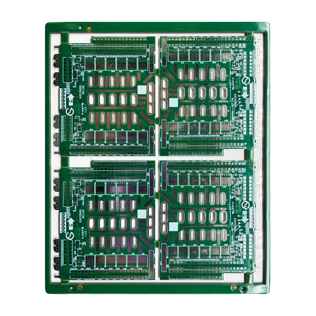
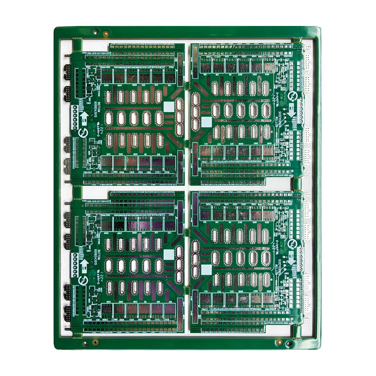
Высоконадежная 8-слойная жесткая печатная плата Обзор продукта & Определение
В сфере высоких скоростей, электронная конструкция высокой плотности, Многослойные печатные платы (Печатные платы) незаменимы. UGPCB 8-слой жесткой печатной платы, построен с существенным 2.0мм толщина доски и 3ОЗ тяжелая медная фольга, спроектирован так, чтобы выдерживать сложные электрические и физические условия. Он служит не только основой для электрического подключения, но и критически важным компонентом, обеспечивающим стабильность устройства и повышенную надежность продукта.. Для применения в промышленном управлении, энергетические системы, или автомобильная электроника, эта плата с высокими техническими характеристиками является оптимальным решением для сложных, высокопроизводительные конструкции.
Основные спецификации
-
Количество слоев: 8-Слой жесткой печатной платы
-
Толщина готовой доски: 2.0мм ±10%
-
Базовый материал: ФР-4, Температура стеклянного перехода (Тг) ≥ 170°С
-
Поверхностная отделка: Выравнивание бессвинцовой пайкой горячим воздухом (ХАСЛ-ЛФ)
-
Медный вес: 3 унции на квадратный фут (≈105 мкм) как для внутреннего, так и для внешнего слоев
-
Припаяя маска & Шелковик: Зеленая паяльная маска LPI, Легенда белой шелкографии
Критические соображения дизайна
При проектировании с использованием этой печатной платы с высокими техническими характеристиками, инженеры должны расставить приоритеты:
-
Тепловое управление: Используйте высокую допустимую токовую нагрузку 3ОЗ тяжелая медь для оптимизации силовых и заземляющих слоев, уменьшение импеданса и нагрева. Используйте термическое моделирование в сочетании с высокой термостойкостью Материал ФР-4 ТГ170.
-
Контроль импеданса & Целостность сигнала: 8-слойный стек обеспечивает эффективное разделение сигнала., власть, и грунтовые слои. Точный расчет и контроль импеданса трассы (например, 50Ом несимметричный, 100Ом дифференциал) важно минимизировать отражения и перекрестные помехи.
-
Механический & Электрическая надежность: The 2.0доска толщиной мм повышает общую жесткость, подходит для применений с вибрацией или вставным напряжением. Для высоковольтных или сильноточных узлов, отрегулируйте ширину дорожки и зазор в соответствии с Стандарты IPC-2221 и 3ОЗ меди вес для обеспечения запаса прочности.
-
DFM (Дизайн для производства): Сотрудничайте с командой инженеров UGPCB заранее, чтобы удовлетворить конкретные требования к тяжелая медная печатная плата и толстая плата печатной платы обработка, такие как параметры сверления и однородность покрытия, обеспечение высокопроизводительного производственного процесса.
Как это работает & Структура
Ан 8-слой печатной платы изготавливается путем ламинирования нескольких проводящих слоев в единое целое с использованием точных процессов, включая визуализацию внутреннего слоя, ламинирование, бурение, и покрытие. Электрические связи между слоями устанавливаются через металлизированные сквозные отверстия (ПТХ), слепые переходы, или скрытые переходные отверстия. Типичный пример стека::
Верхний слой (Сигнал) — Препрег — Л2 (Земля) — Ядро — L3 (Сигнал) — Ядро — L4 (Власть) — Ядро — L5 (Сигнал) — Препрег — Нижний слой (Сигнал)
Этот “бутерброд” структура эффективно изолирует высокоскоростные сигналы, обеспечивает твердые опорные плоскости, и обеспечивает эффективное распределение мощности.
Производительность & Ключевые особенности
-
Превосходные электрические характеристики: 3ОЗ тяжелая медь обеспечивает чрезвычайно низкое сопротивление проводника и отличную токопроводящую способность (более чем в 3 раза больше, чем у стандартной меди на 1 унцию), снижение потерь мощности и падения напряжения.
-
Исключительная тепловая надежность: Высокотемпературный материал FR-4 TG170 выдерживает более высокие температуры эксплуатации и пайки. В сочетании с теплопроводностью тяжелой меди, это значительно повышает долгосрочную надежность в высокотемпературных средах.
-
Повышенная механическая стабильность: The 2.0доска толщиной мм в сочетании с жестким FR-4 обеспечивает превосходную устойчивость к изгибу и вибрации., идеально подходит для тяжелых условий эксплуатации.
-
Высокая надежность паяных соединений: The Поверхностная обработка HASL-LF предоставляет квартиру, копланарная поверхность контактной площадки с отличной паяемостью и увеличенным сроком хранения, соответствует директивам RoHS.
-
Взаимодействие высокой плотности (ИЧР) Возможность: 8-слойная конструкция обеспечивает достаточно места для маршрутизации сложных схем., содействие миниатюризации устройств и функциональной интеграции.
Обзор производственного процесса
Инженерный обзор → Резка материалов (ФР-4 ТГ170) → Визуализация внутреннего слоя & Офорт (3ОЗ) → Оксидная обработка & Ламинирование → Механическое сверление & Меднение → Рисунок внешнего слоя & Покрытие (до 3 унций) → Нанесение паяльной маски (Зеленый ИЛПИ) & Шелковик (Белый) → Бессвинцовая обработка поверхности HASL → Электрические испытания & Заключительная проверка (по стандартам МПК)
Каждый этап включает строгие контрольные точки контроля качества, чтобы гарантировать высоконадежная многослойная печатная плата соответствует точным требованиям заказчика.
Основные приложения & Варианты использования
Эта печатная плата предназначена для высокомощных, высокостабильные приложения:
-
Промышленные системы управления: ПЛК, моторные приводы, и промышленные источники питания, требующие тяжелые медные печатные платы для большого тока.
-
Возобновляемая энергия & Энергетические системы: Солнечные инверторы, Системы ИБП, и модули зарядки электромобилей, рассчитанные на высокую токовую мощность и термическую стойкость..
-
Автомобильная электроника: Бортовые зарядные устройства (OBC), Системы управления батареями (Бит), и DC-DC преобразователи, где ПХБ с высоким Tg важны для измерения температуры под капотом.
-
Телекоммуникационная инфраструктура: Усилители мощности базовых станций и системы резервного питания сети.
-
Высококлассный тест & Измерительное оборудование: Инструменты, требующие стабильной подачи питания и низкого уровня шума..
Классификация продуктов (Согласно стандартам МПК)
-
По количеству слоев: Многослойная печатная плата (>4 слои), в частности 8-слой печатной платы.
-
По жесткости: Жесткая печатная плата.
-
Базовым материалом: Печатная плата FR-4, подмножество: Печатная плата с высоким Tg (Тс ≥ 170°С).
-
Специальным процессом: Тяжелая медная печатная плата (для МПК-2152), Толстая плата печатной платы.
-
По классу приложения: Подходит для Класс МПК 2 (Электронные продукты, предназначенные для специального обслуживания) и Сорт 3 (Высоконадежная электронная продукция) приложения, включая Печатная плата промышленного класса, Печатная плата силовой электроники, и Печатная плата автомобильного класса.


