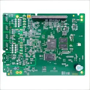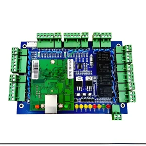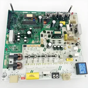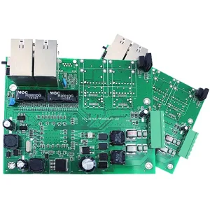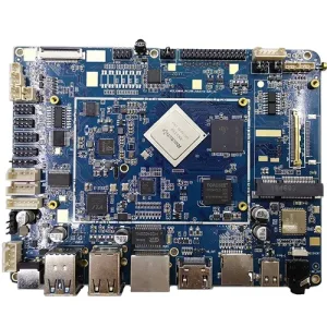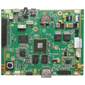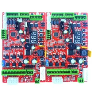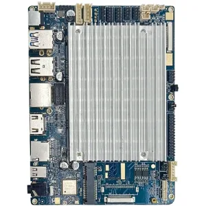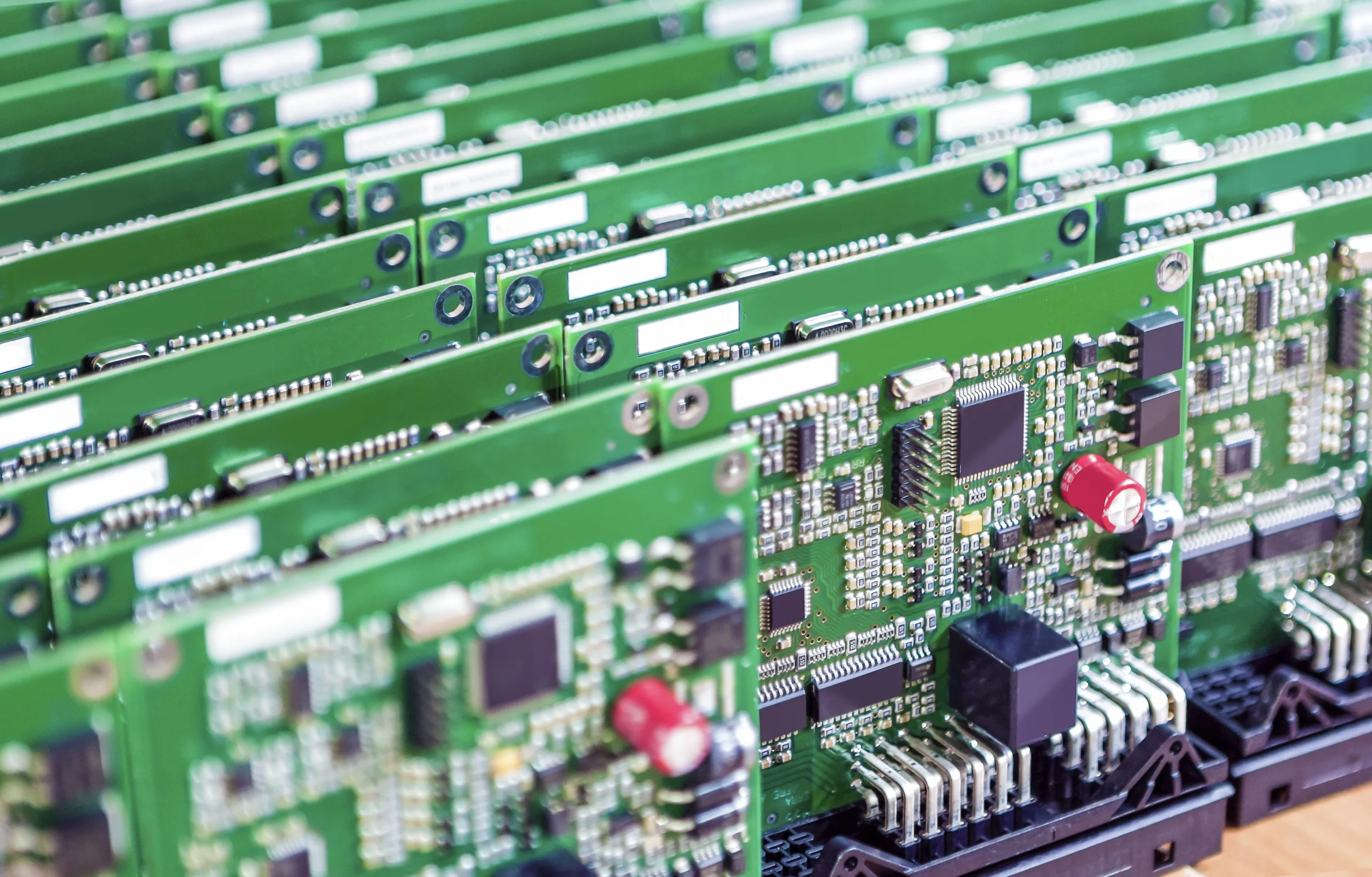
 Двойной встроенный пакет (ОКУНАТЬ), also known as dual inline pin package technology, refers to the packaging of integrated circuit chips in a dual inline form during PCB board factory PCBA immersion operations. В настоящее время, most small and medium-sized integrated circuits use this packaging method, with the number of pins generally not exceeding 100; DIP packaged CPU chips have two rows of pins that need to be inserted into a chip socket with a DIP structure or directly soldered onto a PCB board with the same number of solder holes and geometric arrangement.
The chips in DIP packaging must be carefully inserted and removed from the chip socket to avoid damaging the pins during handling by SMT technicians. DIP packaging structures include: multilayer ceramic DIP, single-layer ceramic DIP, выводная рамка DIP (including glass-ceramic sealed type, plastic package structure type, ceramic low-melting-point glass package type), и т. д..
After DIP component placement, soldering is a process following SMT component placement (except for special cases: plug-in PCB boards only). The processing steps are as follows:
- Pretreatment of PCB components
Pretreatment workshop staff collect materials listed in the BOM according to the material list, carefully check the model and specifications of the materials, then sign for them. They perform pre-production treatment based on models and use fully automatic high-capacity capacitor cutters, triode auto-shaping machines, automatic belt shaping machines, and other shaping equipment for processing.
Требования:
(1) The adjusted width of the component leads must match the width of the positioning holes, with an error of less than 5%;
(2) The distance between component leads and PCB pads should not be too large;
(3) Если этого требует заказчик, parts need to be shaped to provide mechanical support to prevent warping of PCB pads.
- Apply high-temperature adhesive tape to the PCB board—apply high-temperature adhesive tape to block the tinned through-holes and components that must be soldered later;
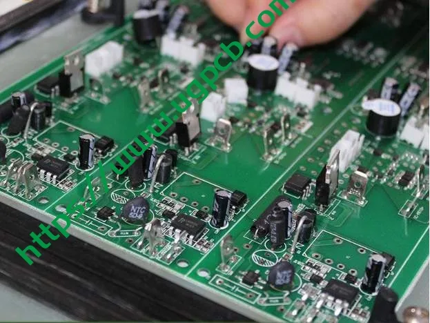
- DIP component insertion personnel must wear anti-static wristbands to prevent static electricity, and perform insertion processing according to the component BOM table and component location diagram. SMT component placement operators must be careful when inserting and removing to avoid errors and omissions;
- For inserted components, operators must inspect mainly to check if any components are inserted incorrectly or missing;
- For PCB boards with no issues in component insertion, the next step is wave soldering. This involves full-automatic PCB board soldering through a wave soldering machine to secure components firmly;
- Remove the high-temperature tape and then inspect. In this step, the main visual inspection is to observe whether the soldered PCB board is well soldered;
- For PCB boards that are not completely soldered, touch-up soldering is performed to prevent issues;
- Post-soldering is a process set for components with special requirements because some components cannot be directly soldered with a wave soldering machine due to process and material limitations, requiring manual completion by operators;
- After all components on the PCB pads are soldered, the PCB board needs to undergo functional testing to ensure all functions are in normal status. If any defects are found in functionality, staff must immediately mark it for pending processing and then repair and retest the PCB board.
We support air conditioning controller DIP processing services. UGPCB - профессиональная универсальная фабрика по обслуживанию печатных плат.. Feel free to learn more about our company.