
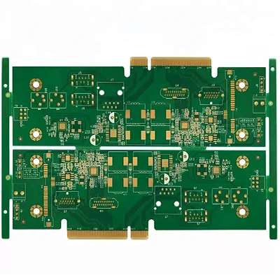
Overview of 6 Layer Golden Finger PCB
The 6 Layer Golden Finger PCB is a high-precision, multi-layered printed circuit board designed for advanced electronic applications. This product combines multiple layers of conductive traces and insulating materials to provide exceptional performance and reliability in various electronic devices.
Определение
А 6 Layer Golden Finger PCB is a type of multi-layer printed circuit board (печатная плата) that features six individual layers of conductive material, разделен изолирующими слоями. Термин “Golden Finger” refers to the specific surface treatment applied to the edges of the board, which involves immersion gold and additional gold plating on the contact fingers.
Требования к дизайну
When designing a 6 Layer Golden Finger PCB, several key requirements must be considered:
- Качество материала: High-quality FR4 material is essential for durability and performance.
- Конфигурация слоя: Six layers are needed to accommodate complex circuitry and signal routing.
- Толщина меди: A standard copper thickness of 1OZ ensures adequate conductivity.
- Обработка поверхности: Immersion gold with additional gold finger plating enhances connectivity and corrosion resistance.
- Трассировка/пространство размеры: A minimum trace/space of 4mil/4mil is required for precise circuit patterns.
- Специальные процессы: The gold finger process with a thickness of 0.1um is critical for reliable edge connections.
Принцип работы
The 6 Layer Golden Finger PCB operates based on the principles of electrical conductivity and insulation. Conductive traces on different layers create pathways for electrical signals, В то время как изоляция слоев предотвращает нежелательные взаимодействия между этими сигналами. The gold finger edges facilitate easy insertion into connectors, ensuring stable and reliable connections.
Приложения
This type of PCB is widely used in applications that require high precision and reliability, такой как:
- High-speed digital circuits
- Телекоммуникационное оборудование
- Advanced computing systems
- Автомобильная электроника
- Медицинские приборы
Классификация
6 Layer Golden Finger PCBs can be classified based on their intended use, такой как:
- Платы по обработке сигналов: Для обработки высокочастотных сигналов в устройствах связи.
- Доски распределения электроэнергии: Управлять источником питания в сложных электронных системах.
- Управляющие доски: For controlling and managing various functions in electronic devices.
Материалы
The primary materials used in the construction of a 6 Layer Golden Finger PCB include:
- Базовый материал: ФР4, Пламя-сногсшибательный стекловолоконной материал, известный своими превосходными диэлектрическими свойствами и механической прочностью.
- Проводящий материал: Медь, используется для проводящих следов.
- Обработка поверхности: Immersion gold and additional gold plating for the gold fingers.
Производительность
Производительность 6 Layer Golden Finger PCB is characterized by:
- Высокая целостность сигнала: Из -за точных графиков/пространственных размеров и качественных материалов.
- Надежная связь: Ensured by the gold finger surface treatment.
- Долговечность: Enhanced by the robust FR4 base material and immersion gold finish.
- Электрическая эффективность: Минимизированная потеря сигнала и помехи из -за оптимизированной конфигурации слоя.
Структура
The structure of a 6 Layer Golden Finger PCB consists of:
- Шесть слоев проводящего материала: Чередование с изоляционными слоями.
- Gold Finger Edges: Plated with a thin layer of gold for enhanced connectivity.
- Protective Layers: Including solder mask and silkscreen for protection and identification.
Функции
Key features of the 6 Layer Golden Finger PCB include:
- Расширенная обработка поверхности: Immersion gold plus gold finger for superior connection quality.
- Высокая точность: With a minimum trace/space of 4mil/4mil.
- Настраиваемые варианты цвета: Доступно в зеленом или белом.
- Стандартная толщина: With a finished thickness of 1.6mm.
Производственный процесс
The production process for a 6 Layer Golden Finger PCB involves several steps:
- Подготовка материала: Выбор и подготовка листов FR4 и медной фольги.
- Наложение слоев: Чередующиеся слои меди и изоляционных материалов.
- Офорт: Удаление лишней меди для формирования желаемого рисунка схемы..
- Покрытие: Applying immersion gold and additional gold finger plating.
- Ламинирование: Объединение слоев под теплом и давлением.
- Бурение: Создание отверстий для компонентов и вайсов.
- Прикладная маска: Защита схемы от припоев мостов и факторов окружающей среды.
- Шелкостная печать: Добавление текста и символов для размещения и идентификации компонентов.
- Контроль качества: Обеспечение печатной платы соответствует всем спецификациям дизайна и стандартам.
Используйте сценарии
The 6 Layer Golden Finger PCB is ideal for scenarios where:
- Высокая целостность сигнала имеет решающее значение.
- Требуются надежные и долговечные соединения.
- Пространственные ограничения требуют компактного и эффективного дизайна.
- Для повышения производительности необходима передовая обработка поверхности.


