

As modern electronic products demand higher integration, меньшие форм -факторы, and improved reliability, traditional rigid PCBs or standalone flexible printed circuits often fall short in complex three-dimensional designs. Жесткие платы offer a solution by combining the mechanical support of rigid boards with the bendability of flexible circuits, making them a preferred choice for high-end electronic applications.
UGPCB specializes in precision Производство печатных плат. This article introduces our flagship product — the Многослойная жесткая гибкая печатная плата (4 Rigid Layers + 2 Flex Layers) — and explains how its structure supports advanced digital product designs.
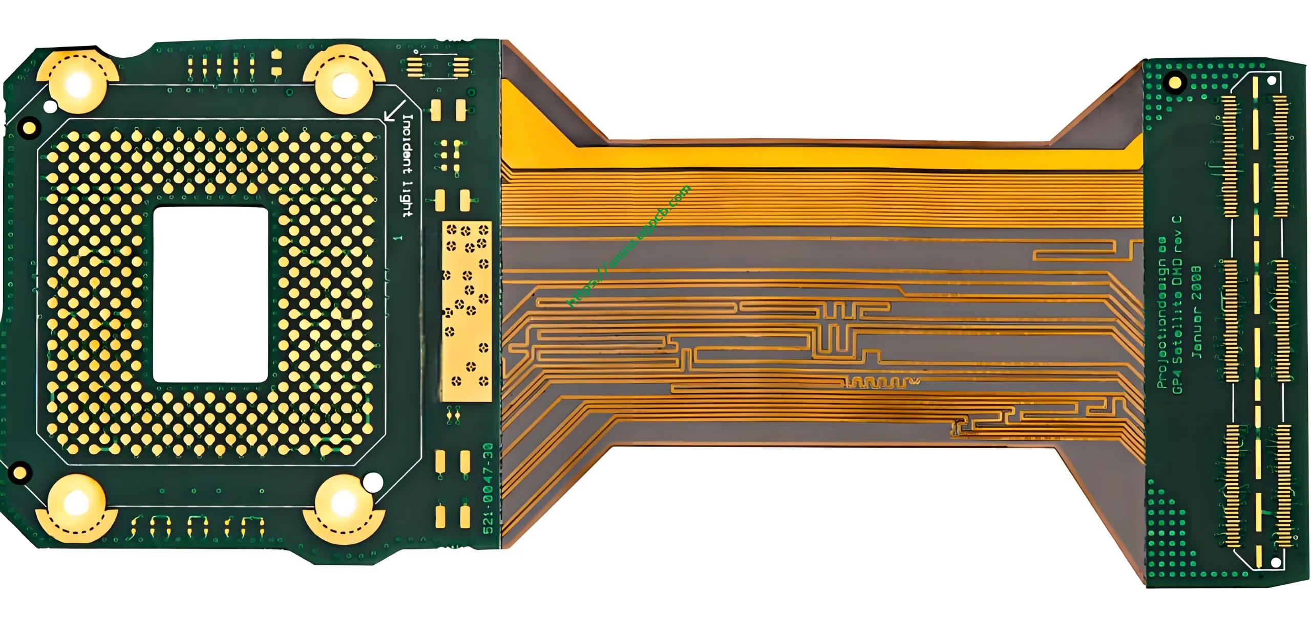
1. What Is a Rigid-Flex PCB?
А жестко-гибкая печатная плата integrates rigid board sections and flexible circuit sections into a single unit through lamination. Unlike conventional assemblies that use connectors to join separate rigid and flexible boards, a rigid-flex PCB establishes seamless electrical connections through plated vias and layer transitions.
This structure provides greater design flexibility. It allows the PCB to be folded or bent inside the device, reducing space usage and eliminating connectors and cables. This improves shock resistance and signal integrity.
2. Обзор продукта: УГКПБ 4+2 Многослойная жесткая гибкая печатная плата
UGPCB offers a rigid-flex PCB with a classic rigid-flex-rigid штабелирование. The key parameters are listed below.
-
Модель: Многослойная жесткая гибкая печатная плата
-
Layer Stack-up: 4 rigid layers + 2 flex layers
-
Материал: ФР-4 (rigid sections) + Полиимид (flex section)
-
Поверхностная отделка: Погружение Золото (СОГЛАШАТЬСЯ)
-
Готовая толщина: 1.0мм (rigid area) + 0.15мм (flex area)
-
Толщина меди: 1 унция
-
Minimum Trace / Космос: 3 мил / 3 мил
-
Приложение: Цифровые продукты
3. Классификация и приложения
Rigid-flex PCBs are generally classified by structure and intended use. UGPCB’s offerings support the following common types:
-
Single-sided or double-sided rigid-flex PCBs – suitable for compact devices such as TWS earphones and smartwatches.
-
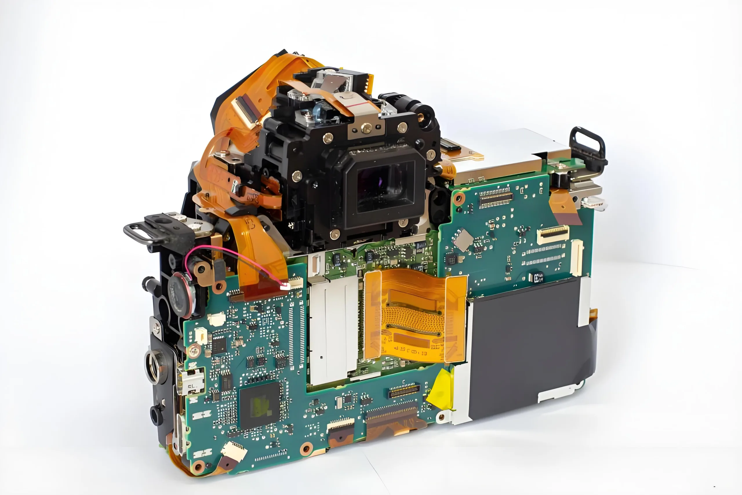
Multi-layer rigid-flex PCBs – UGPCB’s 4 жесткий + 2 flex layer design belongs to this category. It supports high-density component placement and complex routing, making it ideal for smartphones, цифровые фотоаппараты, and similar digital products.
-
Locally reinforced rigid-flex PCBs – used in industrial robotics or foldable displays where high flex life is required.
4. Design Considerations and Working Principle
The operating principle of a rigid-flex PCB is straightforward: rigid sections support components, while flex sections provide bendable interconnects. Однако, successful implementation requires careful design.
Key design practices include:
-
Stack-up symmetry – Symmetrical layer structures prevent warpage caused by thermal stress during lamination.
-
Transition zone treatment – The rigid-flex interface is the most sensitive area. UGPCB follows DFM guidelines by using teardrop pads and tapered traces to reduce stress. Sharp trace angles are avoided to prevent cracking.
-
Flex layer routing – Traces in the flex area should be routed perpendicular to the bend axis. Abrupt direction changes or stacked traces should be avoided to maintain flexibility.
5. Материалы и производительность
The material selection directly affects performance and reliability.
-
Rigid section – FR-4 – Provides mechanical stability and heat dissipation for компоненты such as BGAs and connectors.
-
Flex section – Polyimide (ПИ) – Offers high heat resistance, изоляция, and flex life. When combined with 1 oz rolled annealed copper, it supports dynamic flex applications.
-
Surface finish – Immersion Gold (СОГЛАШАТЬСЯ) – Provides a flat, oxidation-resistant surface suitable for fine-pitch components and ensures reliable solderability.
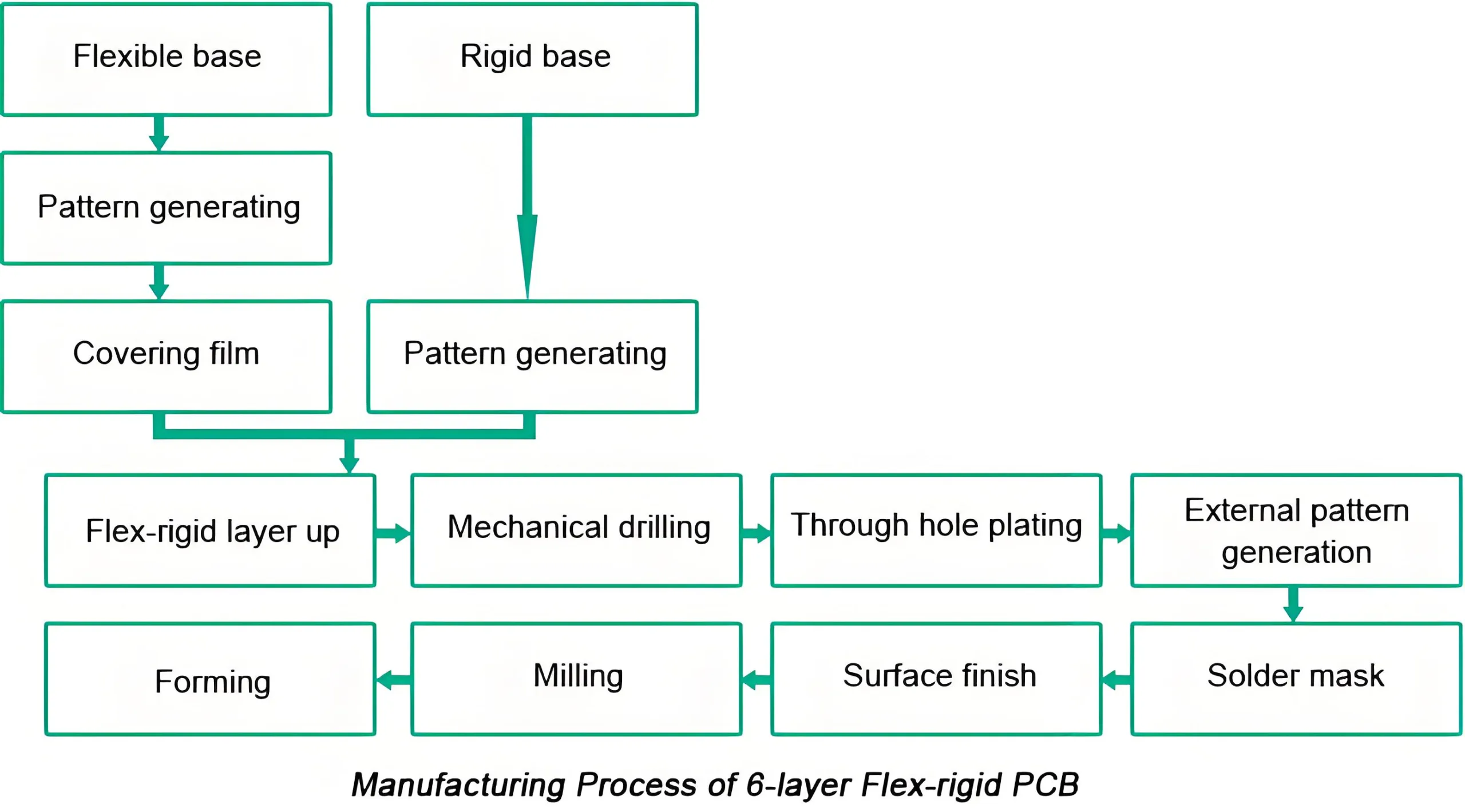
6. Производственный процесс
Producing a high-quality multi-layer rigid-flex PCB requires strict process control. UGPCB follows industry-standard practices to ensure reliability.
-
Material preparation and inner layer imaging – FR-4 and PI materials are cut separately. The inner layer circuits are formed through exposure, разработка, и травление, с 3 mil trace width controlled precisely. AOI inspection verifies quality.
-
Plasma treatment and browning – Plasma cleaning enhances surface activity and improves adhesion between FR-4 and PI before lamination.
-
Ламинирование – The inner layers, препарат, and copper foil are laminated under vacuum and high temperature. Controlling prepreg flow to prevent resin bleed onto the flex area is critical.
-
Drilling and plating – Mechanical and laser drilling create interlayer connections. Electroless copper deposition and electrolytic plating form plated through holes that connect the 4 rigid layers and 2 flex layers.
-
Outer layer imaging and coverlay removal – After outer layer circuit formation, the coverlay over the flex area is precisely removed using laser or chemical methods to free the flexible section.
-
Surface finish and routing – Immersion gold is applied, followed by final routing to the required shape.
7. Ключевые преимущества
UGPCB’s multi-layer rigid-flex PCB offers several benefits:
-
Space efficiency – Replaces two rigid boards and a cable assembly with a single folded unit, saving up to 40% of internal space.
-
Improved reliability – Eliminates connectors and cables, reducing potential failure points. The continuous copper path improves shock resistance.
-
Better signal integrity – Each connector introduces impedance discontinuities. Rigid-flex PCBs provide a continuous transmission path suitable for high-speed signals.
-
Высокая точность – 3 mil trace and space capability, combined with immersion gold finish, supports fine-pitch components and HDI Designs.
-
Lower total cost – Although unit cost may be higher, reduced assembly steps, fewer bill of materials items, and lower labor costs often lead to overall cost savings.
8. Request a Quote
UGPCB provides design support, прототипирование, and volume production. If your project faces space constraints, reliability concerns, or high-speed signal challenges, our team is ready to assist.
Take the next step:
-
Free DFM review – Send your Gerber files. Our engineers will provide manufacturability feedback.
-
Quick quote – Use the inquiry form to share your requirements. A competitive quote will be provided within 24 часы.
-
Technical support – Our application engineers are available to discuss stack-up design or material selection.
[Request a Quote / Get Samples / Contact Support]


