

Für Hochgeschwindigkeits-Leiterplatte (Leiterplatte) Design, Der entscheidende Faktor, der ein robustes Design von einem problematischen unterscheidet, ist für das bloße Auge oft unsichtbar: Der Rückweg des Signals. Jedes Signal, das sich über a ausbreitet Leiterplatte existiert nicht isoliert – es schließt einen Stromkreis, indem es zu seiner Quelle zurückkehrt. Die vom ausgehenden Signal und seinem Rückstrom umschlossene Gesamtfläche definiert die Signalschleife, und die Geometrie dieser Schleife hat einen direkten und entscheidenden Einfluss auf die Signalintegrität (UND) und elektromagnetische Verträglichkeit (EMC) .
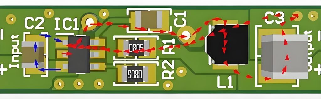
Ingenieurstatistiken zeigen das bis zu 80% von Hochgeschwindigkeitsplatine Fehler entstehen durch Probleme mit der Signalintegrität, Die Sanierung im Spätstadium erweist sich als unverhältnismäßig kostspielig und anspruchsvoll . Dieser Artikel befasst sich mit der Physik von Signalschleifen, quantifiziert ihren Einfluss auf moderne Elektronikdesigns, und bietet umsetzbare Strategien zur Optimierung der Rückwege für Hochgeschwindigkeitssysteme der nächsten Generation.
Grundlegende Schleifenphysik und Rückwegprinzipien
Schleifeneffekte verstehen, Ingenieure müssen zunächst ein Grundprinzip verstehen: Jedes Signal ist ein geschlossener Kreislauf. Strom fließt vom Treiber, durchläuft die Signalspur zum Empfänger, und muss über einen Weg zum Treiber zurückkehren – sei es eine spezielle Bodenebene, ein Motorflugzeug, oder eine andere leitende Route.
Das Verhalten dieses Rückstroms wird durch die Signalfrequenz bestimmt. Für niederfrequente Signale (kHz und darunter), Der Rückstrom folgt dem Weg des geringsten Widerstands, breitet sich über den Leiterquerschnitt aus. Jedoch, Für Hochgeschwindigkeitssignale (über 1 MHz), Das Prinzip ändert sich völlig: Der hochfrequente Rückstrom folgt dem Weg des geringstenInduktivität– kein Widerstand. Aufgrund derHauteffekt, Hochfrequenzströme konzentrieren sich unmittelbar unterhalb der Signalspur auf der angrenzenden Referenzebene (Erde oder Strom), Es entsteht ein eng gekoppeltes Spiegelbild, das die Schleifenfläche minimiert.
Schleifeninduktivität ist die grundlegende physikalische Größe, die das Signal- und EMI-Verhalten bestimmt. Für eine ebene rechteckige Schleife, Die Induktivität kann als proportional zur Schleifenfläche angenähert werden. Diese Beziehung wird durch die Induktivitätsformel für eine rechteckige Schleife erfasst:
L ≈ μ₀ × (A / l)
WoL ist die Schleifeninduktivität (in Henries), μ₀ ist die Durchlässigkeit des freien Raumes (4π × 10⁻⁷ H/m), A ist der Schleifenbereich (in Quadratmetern), und *l* ist der Schleifenumfang (in Metern) . Je größer der Schleifenbereich, desto größer ist die Induktivität, und desto schwerwiegender ist der Leistungsabfall.
Aus der grundlegenden induktiven SpannungsgleichungV = L × (di/dt), Selbst eine geringe Schleifeninduktivität kann in Kombination mit den ultraschnellen Stromtransienten eine erhebliche Rauschspannung erzeugen (di/dt) Charakteristisch für die moderne Hochgeschwindigkeitslogik. Für einen 10 Gbit/s-Signal mit einem 20 PS Anstiegszeit, di/dt kann 10¹¹ A/s überschreiten und so die Induktivität auf Pichenry-Niveau in Rauschen im Millivolt- oder sogar Volt-Niveau umwandeln, das zu Logikfehlern und Massesprüngen führen kann.
EMV-Auswirkungen: Der strahlende Antenneneffekt
Aus EMV-Sicht, Die PCB-Schleife fungiert als Antenne. Je größer der Schleifenbereich, desto effizienter strahlt es elektromagnetische Energie in die Umgebung ab.Die Schleifenfläche ist die dominierende Variable der abgestrahlten EMI-Intensität, und die Kontrolle kritischer Schleifendimensionen ist die effektivste Methode, um Tests zur Einhaltung gesetzlicher Vorschriften zu bestehen.
Branchendaten aus EMV-Debugging-Fällen unterstreichen diese Realität. In einer dokumentierten EMI-Sanierung industrieller Schalttafeln, eine zweischichtige Leiterplatte mit einem ARM Cortex-M7-Prozessor (216 MHz-Hauptfrequenz) mit integrierten CAN-FD- und RS-485-Schnittstellen zeigten deutliche Strahlungsspitzen im Bereich 30–230 MHz. Bei 126 MHz, Der Vorstand hat die CISPR überschritten 32 Klasse-B-Grenze durch 9.2 dBμV/m (gemessen mit der 3-Meter-Methode) . Die Hauptursache wurde auf diskontinuierliche Rückwege zurückgeführt, die eine Umgehung der Schleife und eine Erweiterung des Gebiets erzwangen.
CISPR 32 Grenzwerte werden daraus abgeleitetIEC 61967 Standardanforderungen für integrierte Schaltkreise. Für Hochgeschwindigkeitssignale, die oben betrieben werden 10 MHz, Aufrechterhaltung des Schleifenbereichs unten0.5 cm² wird als Best Practice empfohlen. Wenn sich die Schleifenfläche verdoppelt, Strahlungsemissionen können um bis zu zunehmen6 db– entspricht einer Vervierfachung der Strahlungsleistung. Schleifenbereich unter beibehalten 1 cm² (und darunter 0.5 cm² für Signale größer 100 MHz) stellt sicher, dass die Emissionen innerhalb der meisten gesetzlichen Grenzwerte der Klasse B bleiben.
Jenseits abgestrahlter Emissionen, große Schleifen entstehen Gleichtaktstrahlung wenn hochfrequente Spannungsunterschiede auf der Schleifeninduktivität externe Kabel antreiben und so die Verbindungsverkabelung im Wesentlichen in eine unbeabsichtigte Sendeantenne umwandeln. Das erklärt warum 90% von EMV-Ausfällen im Hochgeschwindigkeitsbereich PCB -Designs können auf unkontrollierte kritische Schleifenbereiche zurückgeführt werden .
Konsequenzen für Signalintegrität und Leistungsintegrität
Der Einfluss der Schleifenfläche auf die Signalintegrität ist ebenso tiefgreifend. Es spielen mehrere Mechanismen eine Rolle:
Impedanzdiskontinuitäten und Reflexionen: Wenn ein Signal zwischen Schichten wechselt (per Übergang) ohne entsprechenden Rückwegübergang, Der Rückstrom ist gezwungen, einen alternativen Weg zu finden – oft über einen viel längeren Weg, der die Schleifenfläche erheblich vergrößert. Diese Pfaddiskontinuität manifestiert sich als lokale Impedanzfehlanpassung, Es kommt zu Signalreflexionen und Klingeln, die die Signalqualität verschlechtern und zu Timing-Verstößen führen.
Crosstalk-Verstärkung: Eine große Signalschleife fungiert als elektromagnetischer Sender, seine Feldenergie in benachbarte Leiterbahnen einkoppelt. B. Taktfrequenzen überschreiten 1 GHz und Anstiegszeiten fallen darunter 50 ps, Der induktive Kopplungskoeffizient zwischen benachbarten Signalpaaren nimmt proportional zur Schleifenfläche zu. Dieser Effekt wird durch gegenseitige Induktivitätsbeziehungen bestimmt.
Bodensprung und gleichzeitiges Schaltrauschen (SSN): Wenn mehrere Hochgeschwindigkeitsausgänge gleichzeitig schalten, Der gesamte Rückstrom fließt durch die Schleifeninduktivitäten ihrer jeweiligen Pfade. Der daraus resultierende Spannungsabfall (V = L × di/dt) manifestiert sich alsBodensprung– eine vorübergehende Spannungsverschiebung zwischen verschiedenen Punkten auf der Grundebene. Gemäß IPC-2141A-Richtlinien, Die Aufrechterhaltung kontinuierlicher Referenzebenen und die Minimierung der Rückweglänge sind grundlegende Anforderungen für Designs mit kontrollierter Impedanz.
Intersymbolinterferenz (ISI) und Bitfehlerrate (BER) Die Verschlechterung ist eine direkte Folge dieser SI-Beeinträchtigungen. Für serielle Hochgeschwindigkeitsverbindungen mit 25 Gbit/s pro Spur (PCIE 5.0), Signalreflexionen unten -15 dB und BER unter 10⁻¹² sind zwingende Anforderungen. Jeder Mikrohenry an unbeabsichtigter Schleifeninduktivität treibt das System in Richtung dieser Leistungsklippen.
Kritische Entwurfsszenarien, die den Schleifenbereich verschärfen
Mehrere gängige PCB-Designpraktiken erzeugen unbeabsichtigt große Signalschleifen. Das Bewusstsein für diese Szenarien ist für die Prävention unerlässlich:
Verstöße gegen die geteilte Ebene: Das Leiten eines Hochgeschwindigkeitssignals über eine Lücke oder einen Spalt in seiner Referenzebene zwingt den Rückstrom dazu, die Diskontinuität zu umgehen. Die daraus resultierende Erweiterung des Schleifenbereichs kann dramatisch sein. Simulationsdaten zeigen, dass, wenn a 10 Gbit/s-Differenzsignal kreuzt a 1 mm GND-Ebene geteilt, Die äquivalente Induktivität des Rückwegs erhöht sich um bis zu400% , mit steigenden abgestrahlten EMI-Spitzen9 dBμV/m .
Unsachgemäßer Ebenenübergang (Durch Nähen): Wenn ein Signal die Schicht wechselt, die benachbarte Referenzebene kann sich gleichzeitig ändern. OhneNähen von Durchkontaktierungen (Erdungsdurchkontaktierungen, die neben den Signaldurchkontaktierungen platziert sind) um einen kontinuierlichen Rückstrompfad bereitzustellen, Der Rückstrom muss seitlich fließen, um den nächstgelegenen Erdungsanschluss zu finden, eine große Schleife erstellen. Für kritische Hochgeschwindigkeitssignale, Die Verbindungslöcher sollten darin platziert werden20 Mils (0.5 mm) des Signals über.
Diskontinuierliche Referenzebenen: Übermäßig aggressiv durch Antipad-Größe, Ausschnitte für Triebwerksflugzeuge, oder übermäßige Hohlräume in der Ebene können zu Diskontinuitäten in der Referenzebene führen, die eine Umgehung des Rückstroms erzwingen. IPC-2141A empfiehlt, alle Hochgeschwindigkeitssignalschichten zur Vervollständigung nebeneinander zu platzieren, kontinuierliche Referenzebenen.
Falsch abgeschlossene Guard Traces: Wachspuren (Zur Abschirmung werden neben empfindlichen Signalen Kupferleiterbahnen angebracht) denen es an ausreichenden Massedurchkontaktierungen mangelt, werden zu nicht abgeschlossenen „schwebenden Antennen“, die mehr Rauschen einkoppeln als sie blockieren können. Für eine effektive Abschirmung, Schutzspuren erfordernIn regelmäßigen Abständen Löcher nähen– typischerweise weniger als 1/20 der Signalwellenlänge voneinander entfernt.
Übergänge der Verbindungsreferenzebene: Bei Board-to-Board- oder Board-to-Cable-Steckverbindern, Die Kontinuität der Referenzebene bricht häufig, Dies erfordert eine sorgfältige Planung der Pinbelegung und die Verwendung dedizierter Erdungspins, um die Integrität des Rückwegs aufrechtzuerhalten.
Praktische Designstrategien zur Schleifenminimierung
Das übergeordnete Gestaltungsprinzip ist klar: niederohmig herstellen, kontinuierliche Rückwege für jedes Hochgeschwindigkeitssignal. Es gibt mehrere bewährte Strategien:
Setzen Sie vollständige Referenzebenen ein: Widmen Sie ganze Schichten der Erdung oder Stromverteilung statt fragmentierter Kupfergüsse. Die Kombination aus Masse- und Stromversorgungsebenen kann bei ordnungsgemäßer Entkopplung als AC-Referenzebenen fungieren.
Optimieren Sie den Ebenenstapel: Platzieren Sie jede Hochgeschwindigkeitssignalschicht direkt neben einer durchgehenden Referenzebene, Minimierung der vertikalen Schleifenhöhe. Diese enge elektrische Kopplung reduziert die Schleifenfläche und steuert die charakteristische Impedanz.
Vermeiden Sie Kreuzungen mit geteilten Flugzeugen: Planen Sie die Platzierung von Komponenten und Signalen, um sicherzustellen, dass Hochgeschwindigkeitssignalspuren niemals Diskontinuitäten in der Referenzebene kreuzen. Wenn eine Überfahrt unvermeidbar ist, Verwenden Sie „Überbrückungsstrategien“ wie das Zusammenfügen von Kondensatoren oder eine lokale Verbindung der Masseebene.
Trace-Länge minimieren: Halten Sie die Hochgeschwindigkeitssignalleitungen so kurz und direkt wie möglich. Jede Einheit Leiterbahnlänge trägt direkt zum Erweiterungspotenzial der Schleifenfläche bei.
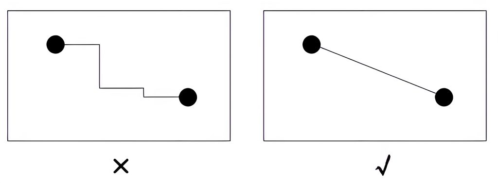
Implementieren Sie das richtige Nähen durch Platzierung: Bei jedem Signalschichtübergang, Platzieren Sie Massedurchkontaktierungen neben den Signaldurchkontaktierungen. Für Differentialpaare, Ortzwei Massedurchkontaktierungen in der Nähe jedes Differential-Via-Paares. Für Single-Ended-Signale, eine angrenzende Masse durch innen 20 mil wird empfohlen.
Nutzen Sie die differenzielle Signalisierung: Differentialpaare erzeugen enge lokale Rückführungsschleifen zwischen den wahren und komplementären Signalen. Dadurch wird die äußere Strahlung reduziert, Differenzsignale erfordern immer noch kontinuierliche Referenzebenen und eine enge Längenanpassung (typischerweise innerhalb 5 Mil für 10 Gbit/s+-Signale).
Verwenden Sie EDA-Simulationstools: Moderne EDA-Plattformen einschließlichTrittfrequenz Sigrity X UndKeysight -Anzeigen bieten Funktionen zur Visualisierung des Rückwegs und zur Analyse des Schleifenbereichs. Die Simulation ermöglicht es Ingenieuren, Diskontinuitäten im Rückweg zu identifizieren und zu beheben, bevor sie mit der Fertigung beginnen.
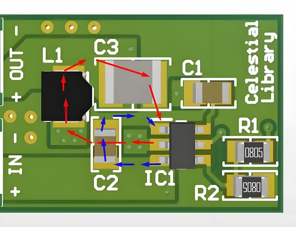
Abschluss
Die bescheidene Signalschleife – die in herkömmlichen schaltplanzentrierten Design-Workflows oft unsichtbar ist – erweist sich als entscheidender Faktor für die Leistung von Hochgeschwindigkeits-PCBs. Ob die Strahlungsemissionen anhand der CISPR-Standards bewertet werden, Quantifizierung der Bitfehlerraten anhand der PCIe-Spezifikationen, oder die Beurteilung der Signalintegritätsmargen, Die Schleifenbereichskontrolle bleibt die verbindende Physik, die all diese Metriken verbindet. Durch Priorisierung der Kontinuität des Rückwegs, Minimierung der Schleifenfläche, und Nutzung moderner EDA-Simulation, Ingenieure können Hochgeschwindigkeits-Leiterplatten entwerfen, die sowohl die Leistungs- als auch die gesetzlichen Anforderungen zuverlässig und kostengünstig erfüllen. Für Organisationen, die diese Designrisiken mindern möchten, mit erfahrenen zusammenarbeiten PCB- und PCBA-Lieferanten gewährleistet die Einhaltung erstklassiger Designpraktiken und eine schnellere Markteinführung.
