
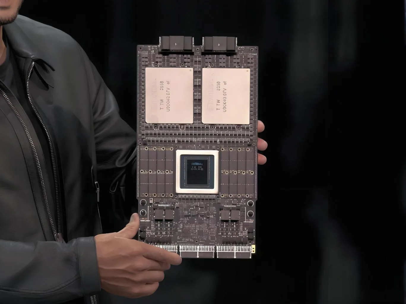
Le fond de panier orthogonal PCB est un composant fondamental pour les clusters informatiques d'IA de nouvelle génération. Doté d'une structure de 78 couches dans un profil de deux centimètres et près d'un mètre carré de superficie, il permet l'interconnexion directe jusqu'à 576 GPU. Ce PCB d'interconnexion haute densité La solution pour l'architecture NVIDIA Rubin Ultra repousse les limites de la fabrication électronique conventionnelle, exigeant une précision sans précédent dans les matériaux, processus, et intégration.
01 Changement architectural: Pourquoi les fonds de panier orthogonaux remplacent les câbles traditionnels
L'évolution vers la technologie de fond de panier orthogonal est une réponse directe aux limites du câblage en cuivre dans les systèmes d'IA massifs.. Dans une configuration haute densité comme l'armoire NVL576, une approche basée sur le câble nécessiterait plus 20,000 câbles individuels, ajoutant un poids important, complexité, et points de défaillance, tout en souffrant également d'une dégradation du signal avec la distance.
En revanche, le “sans câble” fond de panier orthogonal intègre le réseau d'interconnexion directement sur un massif, carte PCB multicouche. Les nœuds de calcul et de commutation se connectent orthogonalement via cette carte unifiée via des plateaux empilés verticalement.. Ce technologie avancée des PCB rationalise le processus d’assemblage, potentiellement améliorer l'efficacité en sur 40%, et résout le défi spatial critique consistant à relier des milliers de composants dans un seul rack.
02 Frontière de la science des matériaux: Le dilemme des performances du M9 et du PTFE
Au cœur de ce multicouche Fabrication de PCB le défi est le matériau lui-même. L'architecture Rubin spécifie un stratifié haute vitesse de qualité M9, choisi pour ses propriétés électriques exceptionnelles: une constante diélectrique ultra faible (Ne sait pas) de 3.0 ou moins et un facteur de dissipation minimal (Df) de 0.0007 ou ci-dessous. Son coefficient de dilatation thermique (CTE) est étroitement contrôlé à ≤7 ppm/°C, ce qui est crucial pour la stabilité dimensionnelle.
Une innovation clé dans les stratifiés M9 est l'utilisation de fibre de quartz (Q-tissu) au lieu de la fibre de verre standard. Bien que cela offre des performances électriques supérieures, ça crée un immense Fabrication de PCB problèmes. La dureté du tissu en quartz réduit considérablement la durée de vie du foret pendant le processus de perçage. Les fabricants doivent donc adopter des forets diamantés coûteux ou des systèmes d'ablation laser., augmentant considérablement les coûts de production.
Pour optimiser davantage les performances électriques dans les chemins de signaux critiques, une approche hybride est souvent utilisée. Les sections du tableau peuvent incorporer du PTFE (Téflon), apprécié pour sa perte ultra faible, malgré son CTE beaucoup plus élevé. Gérer l'écart de dilatation thermique important entre ces différents matériaux - une différence CTE de près de 30x-est un obstacle majeur dans Stratification de circuits imprimés, nécessitant des films de liaison spécialisés et des contrôles de processus précis pour éviter le délaminage ou la déformation sous contrainte thermique.
03 Repousser les limites de la fabrication: Forage, Placage, et alignement des calques
L'échelle physique et le nombre de couches du fond de panier orthogonal créent des Les défis du processus PCB. Une épaisseur de planche de 1-2 cm associé souvent à des diamètres de via >0.2mm se traduit par un rapport hauteur/largeur extrême (épaisseur de la planche par rapport au diamètre du trou) de 100:1 ou plus.
Ce rapport pose de graves problèmes pour le placage de cuivre traversant. À mesure que le rapport hauteur/largeur augmente, il devient exponentiellement plus difficile pour la solution de placage de s'écouler et de déposer le cuivre uniformément en profondeur dans les trous. Avancé placage d'impulsion les techniques sont essentielles pour obtenir une uniformité acceptable, éviter les vides ou les connexions faibles qui pourraient compromettre la fiabilité.
En outre, maintenir Intégrité du signal PCB à hautes fréquences, toute partie inutilisée d'un via (appelé un “bout”) doit être éliminé par un procédé précis contre-perçage processus. Atteindre une tolérance de profondeur de contre-perçage dans ±50 μm sur une planche de cette taille et de cette complexité, c'est un exploit extraordinaire d'usinage de précision, impliquant des CNC systèmes et technologies de mesure.
04 Ingénierie pour la Performance: Intégrité du signal et gestion thermique
Assurer une transmission propre du signal à travers 78 les couches sont primordiales. Cela nécessite des mesures extrêmement serrées contrôle d'impédance, avec des tolérances à l'intérieur ± 5%, la moitié de l'allocation habituelle pour PCB standards. Chaque élément de conception : largeur de trace, espacement, épaisseur diélectrique – doit être méticuleusement calculée et exécutée.
À des débits de données de plusieurs gigabits, des effets physiques comme le effet peau, où le courant circule uniquement à la surface du conducteur, augmenter la résistance et doit être pris en compte dans la conception. De la même manière, empêcher diaphonie entre des traces denses exige de la prudence conception empilable et l'utilisation de plans de masse pour l'isolation.
Gestion thermique des PCB est un défi de co-conception tout aussi crucial. Tandis que les avions en cuivre aident à diffuser la chaleur, le caractère isolant du noyau stratifié (avec une conductivité thermique autour 25 Avec(m · k)) agit comme une barrière. Une dissipation thermique efficace des composants haute puissance tels que les GPU nécessite souvent l'intégration de cadres thermiques métalliques ou de plaques froides directement dans le Assemblage de circuits imprimés, ajouter une autre couche de complexité de conception mécanique et thermique.
05 Chaîne d’approvisionnement et implications sur le marché
L'avènement des fonds de panier orthogonaux représente un changement de valeur significatif dans le Industrie des PCB. Le coût des matériaux et la sophistication technique de ces cartes les placent dans un niveau premium, créer de hautes barrières à l’entrée. Les matériaux spécialisés comme le tissu de quartz ont une offre mondiale limitée, concentrer la capacité de fabrication entre quelques leaders Fournisseurs de PCB.
Pour les entreprises qui peuvent maîtriser cela technologie avancée des PCB, l'opportunité est substantielle. À mesure que les architectures de serveurs IA évoluent pour adopter ce facteur de forme, la demande pour ces cartes sophistiquées devrait augmenter, créer un nouveau segment à forte marge dans le segment haute fréquence MATÉRIAUX PCB et marché manufacturier. Cela stimule l’innovation tout au long de la chaîne d’approvisionnement, des producteurs de stratifiés aux fabricants d'équipements.
06 La trajectoire future de la technologie des PCB
Le fond de panier orthogonal est un point de repère dans Développement de PCB, mais ce n'est pas le point final. L'industrie continue de rechercher des matériaux de nouvelle génération, tels que les hydrocarbures modifiés et autres résines à faibles pertes, pour pousser encore plus loin la perte de signal et les débits de données.
La convergence de la technologie de l'emballage et des PCB s'accélère également. Des concepts comme l'intégré composants et PCB de type substrat (Orthophoniste) brouiller les frontières entre la fabrication traditionnelle de cartes et le conditionnement de semi-conducteurs, visant à créer des systèmes toujours plus intégrés et efficaces. Le succès dans le domaine des fonds de panier orthogonaux fournit l'expertise fondamentale nécessaire à ces avancées futures.
La maîtrise du fond de panier orthogonal est plus qu'une réussite de fabrication; c'est une déclaration de capacité technologique à l'ère de l'IA. Cela nécessite une intégration transparente de la science des matériaux, ingénierie de précision, et la réflexion conceptuelle au niveau du système. Pour Fabricants de PCB et leurs clients, relever ces défis extrêmes est la voie définitive pour réaliser le prochain bond en avant en matière de performances informatiques.
