
With the rapid growth of 5G communication, radar à ondes de millimètres, et communications satellites, Conception de circuits imprimés engineers face a classic dilemma. Using high-end high-frequency materials like Rogers RO4350B for the entire board gives excellent electrical performance but becomes too expensive. Using standard FR4 for the whole board saves cost, but high-frequency signal loss is high and the dielectric constant is unstable.
UGPCB’s Rogers RO4350B+FR4 high frequency hybrid board solves this problem perfectly. This article covers product overview, design guidelines, principes de travail, paramètres techniques, manufacturing process, and applications. It provides a reliable reference for RF engineers and purchasing decision-makers.

1. Présentation du produit: What is a Rogers RO4350B+FR4 High Frequency Hybrid PCB?
1.1 Définition
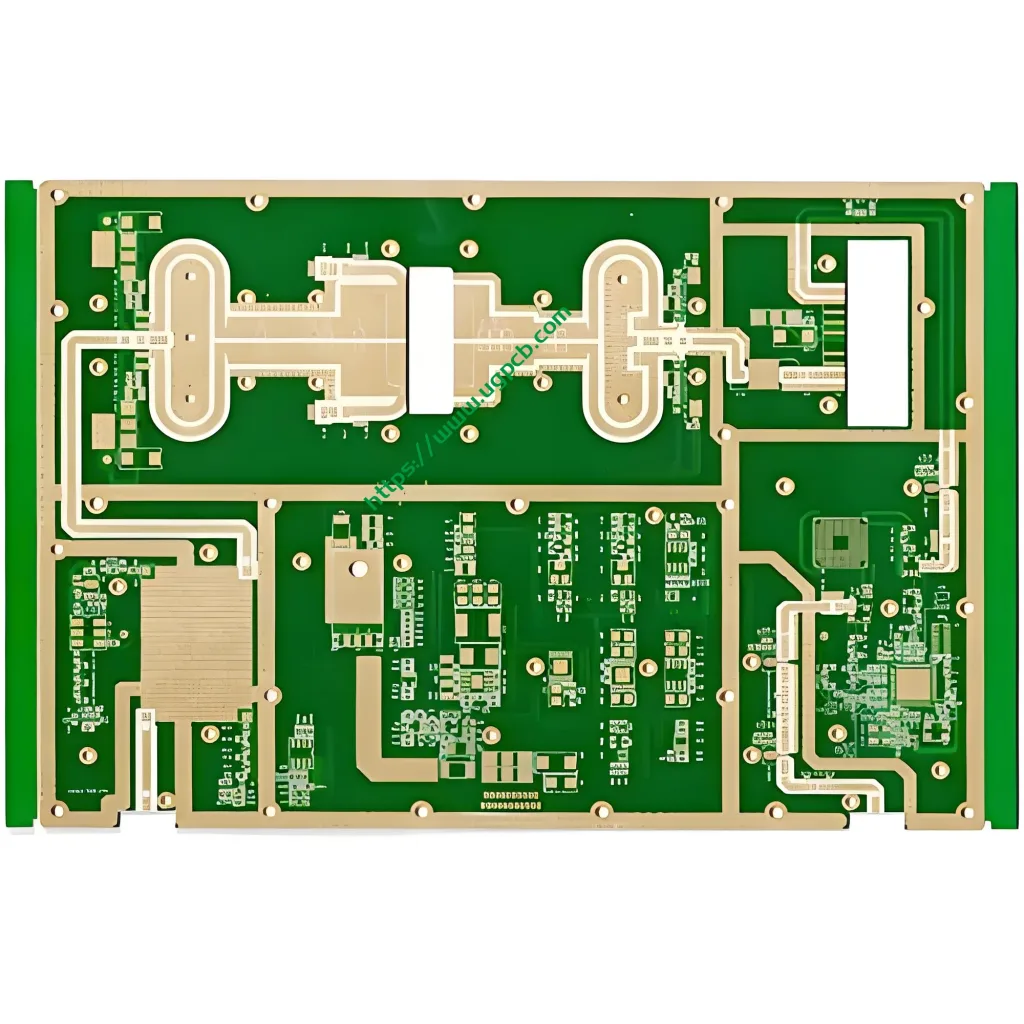
A Rogers RO4350B+FR4 high frequency hybrid PCB uses both Rogers RO4350B high frequency laminate and standard FR-4 epoxy glass fabric on the same circuit board. UGPCB’s product uses a 4-layer symmetrical stack-up: two outer layers of Rogers RO4350B for RF signal routing, and two inner layers of FR4 for power distribution and ground planes. This creates a standard “signal – ground – power – signal” empilement.
1.2 Core Value Proposition
Ce PCB hybride solution delivers precise balance between performance and cost. It uses high-performance Rogers material only on the outer layers where high frequency signals travel. It uses low-cost FR4 on the inner layers. This significantly reduces total Fabrication de PCB cost without sacrificing RF performance. Industry estimates show a 30%–50% material cost reduction compared to a full Rogers board.
2. Key Technical Parameters (Rogers Official Data & UGPCB Specs)
| Paramètre | Valeur | Conditions d'essai / Standard | Source |
|---|---|---|---|
| Material combination | 2 layers Rogers RO4350B + 2 couches FR4 | 4-layer symmetrical stack-up | UGPCB |
| Finished board thickness | 1.2 mm | - | UGPCB |
| Épaisseur de la feuille de cuivre | 1 OZ outer / 1 OZ inner | Finished copper | UGPCB |
| Épaisseur diélectrique | 0.508 mm | - | UGPCB |
| Dielectric constant Dk | 3.48 ± 0.05 @ 10 GHz | IPC-TM-650 | Rogers official datasheet |
| Dissipation factor Df | 0.0037 @ 10 GHz | IPC-TM-650 | Rogers official datasheet |
| Thermal conductivity λ | 0.69 W/m·K @ 50°C | ASTM D5470 | Rogers official datasheet |
| Flammability rating | UL 94 V-0 | UL 94 | Rogers official datasheet |
| Volume resistivity ρ_v | 1.2 × 10¹⁰ Mohm·cm | - | Rogers official datasheet |
| Surface resistivity ρ_s | 5.7 × 10⁹ Mohm | - | Rogers official datasheet |
| Axe Z CTE | 32 ppm/°C | -55°C to 288°C | Rogers official datasheet |
| Densité | 1.9 gm/cm³ | - | Rogers official datasheet |
3. Design Guidelines for Rogers RO4350B+FR4 Hybrid PCBs
Engineers must focus on these key technical points when designing a hybrid PCB with Rogers RO4350B and FR4.
3.1 Impedance Matching Design
The dielectric constant difference between RO4350B and FR4 is significant. RO4350B has Dk = 3.48 à 10 GHz, while standard FR4 has Dk between 4.2 et 4.8. Signal line impedance changes depending on the material layer.
Example for a 50Ω microstrip line:
- On RO4350B layer (NSP = 3,48, 1 Cuivre OZ), 50Ω trace width ≈ 0.4 mm
- On FR4 layer (Dk≈4.5, same copper), 50Ω trace width ≈ 0.25 mm
Design recommendations:
- Keep high-frequency signal traces entirely within the RO4350B signal layers. Avoid crossing material boundaries where impedance changes suddenly.
- If a cross-layer transition is unavoidable, use tapered trace width at the RO4350B-FR4 boundary. Or use electromagnetic simulation to minimize signal reflection caused by the sudden Dk change.
3.2 Symmetrical Stack-up Design
Preventing board warpage is a core concern in hybrid stack-up design. RO4350B has X/Y axis CTE of about 10/12 ppm/°C, while FR4 has about 16 ppm/°C. This mismatch is significant.
UGPCB strictly follows a symmetrical stack-up principle. We use a copper thickness distribution of:
1 OZ RO4350B (top signal) - 0.5 OZ FR4 (sol) - 0.5 OZ FR4 (pouvoir) - 1 OZ RO4350B (bottom signal).
This makes thermal stress distribution even during lamination and greatly reduces warpage risk.
3.3 Transmission Line Selection for RF PCBs
For high frequency applications, we recommend grounded coplanar waveguide (GCPW) instead of traditional microstrip lines. GCPW places dense via fences on both sides of the signal line. This effectively shields crosstalk and reduces electromagnetic interference. It works especially well for 5G millimeter-wave and 77 Radar automobile GHz.
3.4 Drilling and Desmear Process
UGPCB uses drilling parameters recommended by Rogers for RO4350B. We also optimize the desmear process for the mixed material. FR4 resin residue can cause rough hole walls. Donc, we extend plasma desmear time by about 30% compared to pure Rogers boards. This ensures clean hole walls and high-quality metallization.
4. Working Principle and Electrical Performance
4.1 Stabilité constante diélectrique
RO4350B belongs to Rogers’ RO4000 series hydrocarbon/ceramic filled laminates. Its key feature is tight dielectric constant tolerance of ±0.05 over a wide frequency range. The Dk variation with temperature is only +50 ppm/°C (moins que 0.4% change from -50°C to 150°C). This ensures stable operation of communication equipment across the full temperature range.
4.2 Signal Loss Analysis
À 10 GHz, the dissipation factor Df of RO4350B is 0.0037. This is much lower than that of ordinary FR4 at the same frequency (Df ≈ 0.015–0.025). This low-loss property maintains signal integrity over long distances for millimeter-wave signals. In the 5G millimeter-wave band (au-dessus de 24 GHz), UGPCB’s hybrid board typically shows insertion loss below 0.5 dB/inch and return loss above 15 db (users should verify with a VNA on their specific design).
4.3 Thermal Conductivity and Thermal Management
RO4350B a une conductivité thermique de 0.69 W / m · k, about twice that of ordinary FR4 (≈0.3 W/m·K). This allows the hybrid high frequency PCB to efficiently conduct heat from high-power devices like power amplifiers (Pennsylvanie) to copper layers and thermal vias, then spread it through the FR4 inner copper planes. This gives an excellent thermal management solution for RF power amplifier modules.
5. Classement du produit
| Classification Dimension | Catégorie |
|---|---|
| Material type | Hybrid dielectric PCB / High frequency hybrid laminated board |
| Layer count | 4-carte PCB multicouche de couche |
| Application frequency | RF/microwave PCB, covering up to millimeter-wave bands (79 GHz max) |
| Manufacturing process | Mixed lamination multilayer |
| Flammability rating | UL 94 V-0 rated PCB |
UGPCB manufactures and tests according to IPC-6012 (Qualification et spécifications de performances pour les cartes imprimées rigides) and IPC-4101 (Specification for Base Materials for Rigid and Multilayer Printed Boards).
6. Stack-up Structure of the 4-Layer 1.2mm Hybrid PCB
UGPCB’s 1.2mm thick 4-layer Rogers RO4350B+FR4 high frequency hybrid board uses a standard symmetrical stack-up:
- L1 (Top layer): Rogers RO4350B, 1 OZ finished copper – RF signal layer
- L2 (Couche 2): FR4, 1 OZ copper – Ground plane
- L3 (Couche 3): FR4, 1 OZ copper – Power distribution / low-frequency control signals (avion à moteur)
- L4 (Bottom layer): Rogers RO4350B, 1 OZ finished copper – RF signal layer
Total dielectric thickness is 0.508 mm. Finished board thickness is 1.2 mm.
Finition superficielle: ACCEPTER (Or par immersion au nickel autocatalytique) – meets high-reliability soldering and oxidation resistance requirements.
7. Analyse des matériaux
7.1 Rogers RO4350B High Frequency Material
RO4350B is a composite laminate of hydrocarbon resin, charge céramique, and woven glass fabric. Its main advantages include:
- Process compatibility: Fabrication is nearly the same as FR-4. No special hole wall treatment needed (unlike PTFE materials). Manufacturing cost is much lower than traditional microwave laminates.
- UL 94 V-0 cote d'inflammabilité: Suitable for active devices and high-power RF designs.
- CTE à faible axe z (32 ppm/°C): Ensures high reliability of plated through holes (PTH) in multilayer circuits.
7.2 FR4 Substrate
We use high Tg FR4 material (Tg ≥ 170°C) to match the thermal processing window of Rogers RO4350B. FR4 acts as the power and ground layers in the hybrid board. Its cost is only 1/5 à 1/3 that of Rogers material, greatly reducing total PCB manufacturing cost.
8. Manufacturing Process for Hybrid High Frequency PCBs
UGPCB follows a strict quality control process for high frequency hybrid boards:
- Cutting and browning: Apply browning treatment to RO4350B cores and FR4 cores to improve layer adhesion.
- Inner layer circuit patterning: Create ground and power layer patterns on inner FR4 layers.
- Hybrid lamination (critical step): Use a stepped temperature lamination profile (par ex., 120°C → 170°C → 220°C). Select prepregs compatible with both materials. Strictly control ramp rate and press time to avoid delamination or voids.
- Drilling and desmear: Use Rogers-recommended drilling parameters. Increase plasma desmear time by about 30% for mixed material to ensure clean hole walls.
- Plated through hole (PTH): Bake boards at 150°C for 2 hours before electroless copper deposition to compensate for moisture absorption differences (FR4 water absorption >0.1%, RO4350B <0.02%).
- Outer layer circuit patterning: Form signal traces on top and bottom RO4350B layers.
- Solder mask and surface finish: No solder mask on antenna openings. Use ENIG (Or par immersion au nickel autocatalytique).
- Electrical test and reliability inspection: 100% essai électrique, Zone d'intérêt optical inspection, X-ray layer-to-layer alignment check, plus flatness measurement and correction before shipment.
9. Performance and Features of the Hybrid PCB
9.1 Core Performance Values
- Dielectric constant Dk: 3.48 ± 0.05 @ 10 GHz (Rogers official)
- Dissipation factor Df: 0.0037 @ 10 GHz
- Conductivité thermique: 0.69 W/m·K @ 50°C (ASTM D5470)
- Plage de température de fonctionnement: -50°C à +150°C
- Flammability rating: UL 94 V-0
- Résistivité volumique: 1.2 × 10¹⁰ Mohm·cm
- Résistivité superficielle: 5.7 × 10⁹ Mohm
- Densité: 1.9 gm/cm³
9.2 Product Features (Why choose this 4-layer RF microwave PCB)
- ✅ Best performance-cost balance: Saves 30%–50% material cost vs. full Rogers solution.
- ✅ Constante diélectrique stable: ±0.05 tight tolerance, minimal variation with temperature/frequency.
- ✅ Low-loss transmission: Df=0.0037 @ 10 GHz, excellent millimeter-wave signal integrity.
- ✅ FR4-compatible process: No special hole wall treatment, high manufacturing efficiency.
- ✅ Good thermal management: Conductivité thermique 0.69 W / m · k, effective heat dissipation.
- ✅ V-0 cote d'inflammabilité: Meets UL 94 V-0 safety standard.
- ✅ Flexible customization: 1.2 mm épaisseur, supports multiple surface finishes.
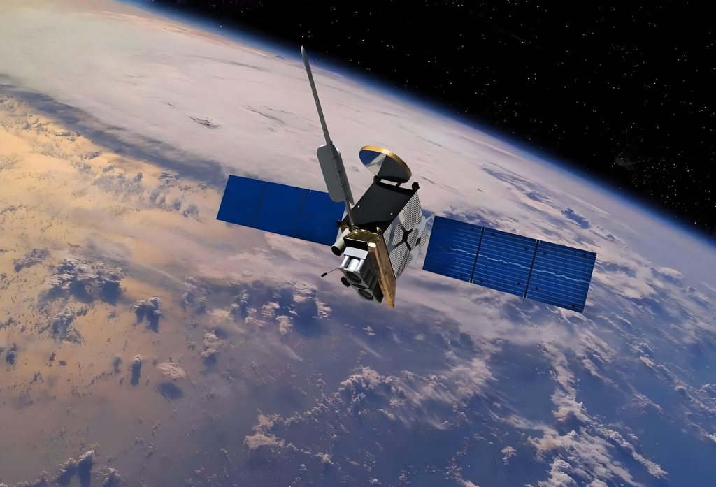
10. Applications of Rogers RO4350B+FR4 High Frequency Hybrid PCBs
Thanks to excellent RF performance and cost advantages, this hybrid PCB serves many key fields:
10.1 5G infrastructure de communication
- 5G macro base station antenna boards and power amplifier modules (PA layer uses RO4350B, power/ground layers use high Tg FR4 with 2+ oz thick copper)
- Microwave point-to-point (P2P) connection equipment
- Satellite communication ground terminal LNBs
10.2 Automotive Electronics and Autonomous Driving
- 77 GHz / 79 GHz automotive millimeter-wave radar – core sensing component for ADAS and autonomous driving; requires AEC-Q100 qualification
- Vehicle-to-everything (V2X) module de communication
- 24 GHz blind spot detection radar sensors
10.3 Modules frontaux RF
- Amplificateurs de puissance (Pennsylvanie) and low noise amplifiers (LNA) modules
- RF transceiver front-ends
- Millimeter-wave phased array antenna T/R modules
10.4 Équipements industriels et médicaux
- RFID readers and tags
- High frequency signal processing circuits in medical imaging (IRM, CT)
- Precision inspection and measurement instruments
10.5 IoT and Consumer Electronics
- 5G CPE (customer premises equipment)
- Wireless inductive communication systems
- Wi-Fi 6E/7 antenna modules
11. Why Choose UGPCB for Your High Frequency Hybrid PCB?
UGPCB has mature process systems and rich practical experience in high frequency hybrid board fabrication.
- 🔧 Mature process: Master core hybrid lamination techniques – stepped press cycles, plasma desmear, layer-to-layer alignment control.
- 📋 100% tested: Full process quality control, 100% essai électrique, AOI optical inspection, X-ray alignment verification.
- ⚡ Fast delivery: Sufficient raw material stock of RO4350B and FR4 ensures controllable lead times.
- 📞 Professional technical support: One-stop engineering support from stack-up design consulting to impedance simulation.
- 🏭 Extensive manufacturing experience: Many years in PCB haute fréquence production, serving global customers.
Get a Quick Quote & Technical Consultation
UGPCB offers free impedance design consulting and high-precision sample manufacturing.
📧Send inquiries to: sales@ugpcb.com
📝Request a fast quote: Please provide Gerber files, spécification matérielle (RO4350B+FR4), nombre de couches (4 couches), épaisseur du panneau (1.2mm), épaisseur du cuivre (1 once), and any other process requirements
🔧Technical support: Contact UGPCB’s engineering team for stack-up design, impedance matching calculations, and hybrid lamination process parameters.
💡 Inquiry tip: To ensure an accurate quote, include complete Gerber files (with drill layer), stack-up requirements, minimum trace width/spacing, and surface finish specification.
Clause de non-responsabilité & Data Accuracy Statement
All technical parameters in this document have been manually verified against the Rogers official datasheet (2025-2026 edition), Normes IPC, and UL certification documentation. Core data – Dk=3.48 (@ 10 GHz), Df=0,0037 (@ 10 GHz), conductivité thermique 0.69 W / m · k (@50°C per ASTM D5470) – come directly from the Rogers RO4350B datasheet. This article follows fair use guidelines for citation and has been reasonably adapted and restructured.
© 2026 UGPCB. All Rights Reserved. | High Frequency Hybrid PCB Design & Manufacturing Expert


