
5G 통신으로서, 항공우주, and high-end medical electronic devices advance rapidly, product internal space becomes increasingly compact, while demanding higher signal transmission stability and reliability. Traditional rigid PCB or cable connections can no longer meet these complex design requirements. UGPCB 8-레이어 Rigid-Flex PCB, with its unique rigid-flex integrated structure, perfectly solves the challenges of three-dimensional assembly and high-density interconnection. It provides an ideal “rigid and flexible” carrier for your designs.
What is a Rigid-Flex PCB?
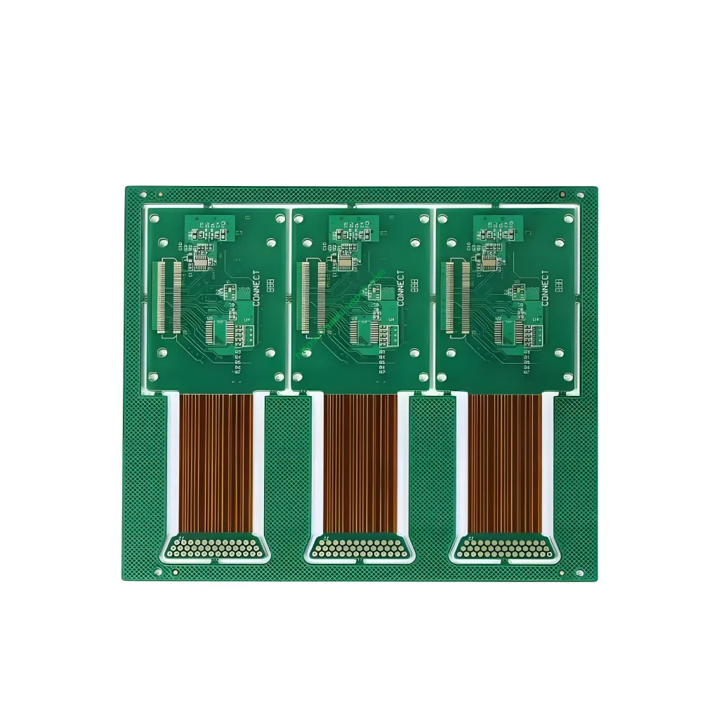
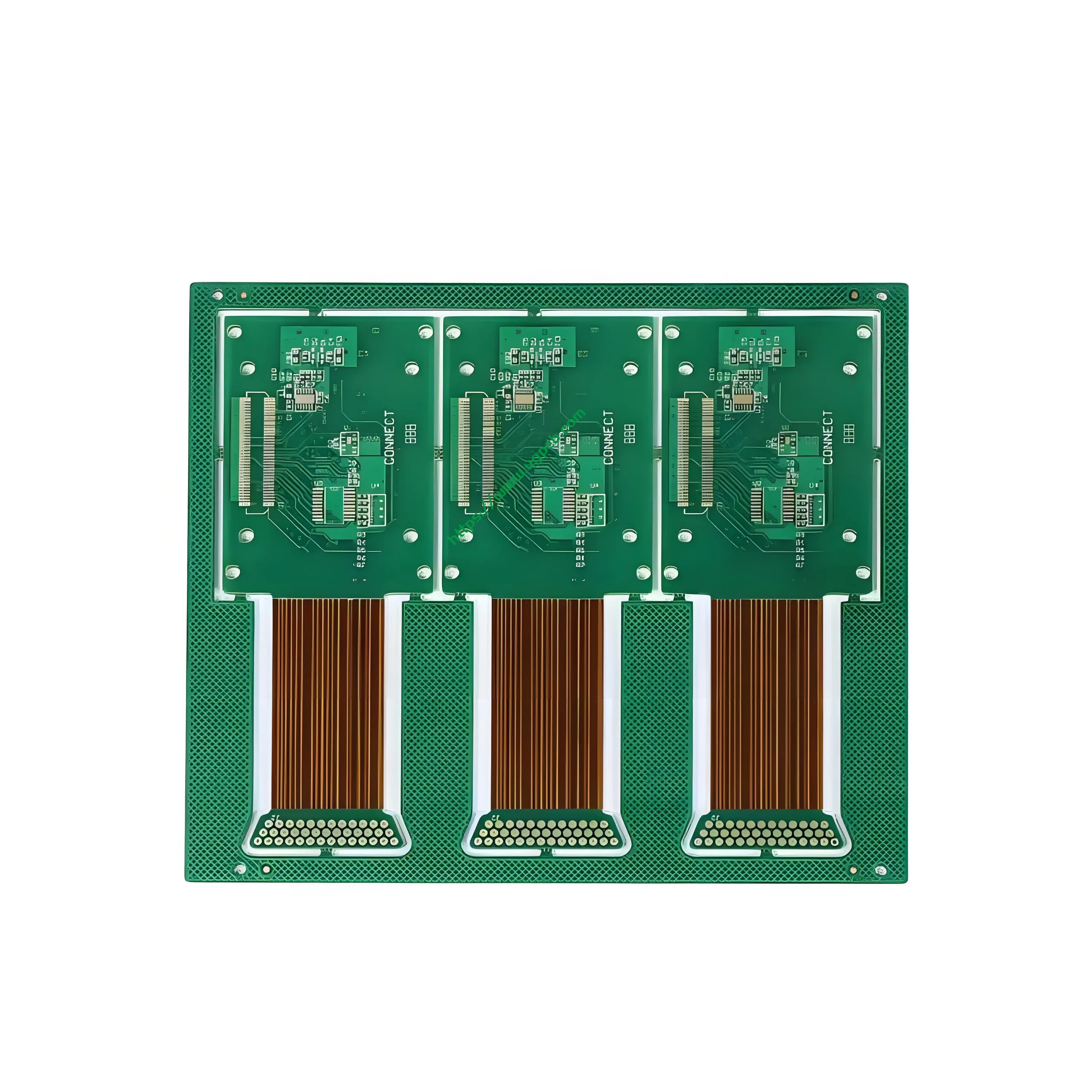
에이 리지드 플렉스 PCB is a composite circuit board formed by combining 유연한 인쇄 회로 그리고 rigid printed circuits through a lamination process, according to specific circuit design requirements.
It is not a simple physical overlay. 대신에, it integrates the bendable and foldable characteristics of flexible circuits with the high mechanical strength and load-bearing capacity of rigid circuits. In UGPCB’s product, we achieve seamless electrical interconnection between 4 rigid layers and 4 flexible layers through precise stack-up design. This allows a single circuit board to securely mount components while bending and navigating through tight spaces.
디자인 하이라이트: Precise 8-Layer Rigid-Flex Structure
To meet the stringent demands of communication equipment for signal integrity and mechanical stability, UGPCB’s product adopts a symmetrical 8-층 (4R+4F) structure design.
-
Stack-up Control: Four rigid layers (using FR-4) host complex logic devices, while four flexible layers (using polyimide) enable signal connections across different areas. This design effectively avoids signal attenuation and assembly errors caused by connectors and cables.
-
임피던스 매칭: At the rigid-flex interface, we implement smooth trace transitions to ensure impedance continuity, 이는 매우 중요합니다. 고속 커뮤니케이션 애플리케이션.
-
Bending Radius Consideration: Considering the bending stress of multi-layer structures, our design ensures the bend radius of the flexible area is significantly larger than the minimum allowable value (typically more than 10 times the total thickness) to prevent copper foil fracture.
Working Principle and Structure
The working principle of this 8-layer rigid-flex PCB is based on its unique physical structure:
-
엄격한 지역: The four rigid layers mainly provide mechanical support for components, such as mounting main control chips, 전원 모듈, 및 커넥터. Internal circuits are interconnected through plated through-holes.
-
유연한 지역: The four flexible layers act as the “electrical spine,” responsible for transmitting data between different modules of the device (예를 들어, between the main control board and display panel or RF front-end). Due to the use of 폴리이미드 기판, they can bend into various shapes to fit the device enclosure.
-
Interconnection Interface: The junction between rigid and flexible sections is specially treated (예를 들어, teardrop connections, stepped transitions) to ensure electrical connection reliability during dynamic bending.
Core Materials and Performance Advantages
UGPCB selects top-grade materials for this product to ensure excellent performance in harsh environments:
-
기판: Combination of FR-4 그리고 폴리이미드. FR-4 provides mechanical strength in rigid areas, while PI offers exceptional heat resistance, 화학 저항, and flex life in flexible areas.
-
구리 포일: The entire board uses 1 온스 구리 두께. For flexible areas subject to dynamic bending, the use of rolled annealed copper ensures excellent bending endurance.
-
표면 마감: 이머젼 골드 ~와 함께 3µ” gold thickness. The thick gold layer provides superior surface flatness and contact reliability, particularly suitable for contacts requiring frequent insertion/withdrawal or long-term stable connection in communication equipment.
제조 공정 및 품질 관리
To achieve high-precision 4mil/4mil traces and complex 8-layer structures, UGPCB follows a strict standardized production process:
-
Inner Layer Preparation: Fabricate four rigid inner layers and four flexible inner layers separately. 사용 마이크로 에칭 to treat the flexible board surface, ensuring trace adhesion.
-
Window Opening and Brown Oxide: Precisely cut windows in the bonding sheets for rigid and flexible areas to prevent excessive resin flow that could affect the flexibility of the flex areas.
-
라미네이션: 사용 no-flow prepreg to bond rigid and flexible sections together under high temperature and pressure in a single or sequential lamination process, ensuring strong bonding without voids.
-
시추 및 도금: 사용 엑스레이 교련 to ensure 정렬 정확도 of multiple layers. Then drill and remove smear, followed by electroless copper plating to achieve interlayer connection.
-
라우팅: Use laser or controlled-depth routing to precisely mill away excess material in flexible areas, releasing the flexible sections.
Product Classification and Applications
구조적으로, this product belongs to multi-layer rigid-flex boards (유형 3 또는 4 under IPC-6013 standards).
Primary Application Scenarios:
-
통신 장비: Such as base station antenna elements, board-to-board connections within RRU/BBU, high-frequency signal transmission modules.
-
산업 제어: Circuit connections in robotic arms, connections between industrial PC hard drives and motherboards.
-
의료 전자 장치: 내시경, 보청기, and various miniaturized, high-reliability portable monitors.
-
자동차 전자: Steering wheel control button boards, in-vehicle camera module connections.
Why Choose UGPCB’s 8-Layer Rigid-Flex PCB?
In the manufacturing of complex multi-layer rigid-flex boards, 층간 정렬, resin flow control, and flexible area protection are three major challenges. UGPCB, with its advanced laser alignment systems 그리고 controlled-depth routing machines, maintains interlayer registration tolerance at a leading industry level.
Whether you are designing next-generation communication base stations or developing sophisticated medical equipment, UGPCB 8-layer rigid-flex PCB is a trustworthy choice. It will help your product achieve infinite possibilities within limited space.
Ready to Turn Your Innovative Design into Reality?
Don’t let complex PCB manufacturing processes slow down your development. UGPCB offers one-stop service from engineering review to mass production.
Upload Your Gerber Files Now for a free DFM analysis report and highly competitive quote! Our engineers will provide the optimal manufacturing solution within 24 시간.
[Click Here to Get a Quote]
UGPCB – Focused on High-Precision Circuit Board Manufacturing, Delivering a Reliable Core for Your Products!


