
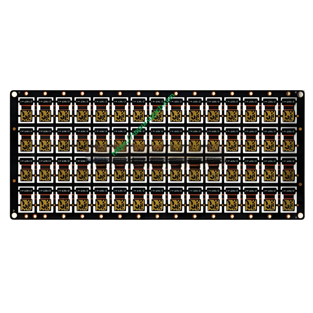
As consumer electronics shrink and automotive electrification accelerates, 글로벌 리지드 플렉스 PCB market reached US$2.462 billion in 2025. Experts forecast it will reach US$3.471 billion by 2032, growing at a 5.1% cagr. Designers face mounting challenges with high-speed data transmission, extreme space constraints, and three-dimensional heterogeneous integration. UGPCB responds with a purpose-built 리지드 4L + Flex 2L rigid-flex PCB solution for high-performance camera modules. This solution features NiPdAu (electroless nickel/palladium/immersion gold) 표면 마감, 3mil precision trace routing, and 0.2mm microvia capability. It ensures lossless MIPI high-speed signal transmission. The integrated rigid-flex interconnection also simplifies assembly workflow. This rigid-flex PCB delivers both high performance and high reliability for mobile imaging and embedded vision systems. 아래에, we provide a comprehensive technical analysis of this product.
1. What Is a Rigid-Flex PCB?
에이 리지드 플렉스 PCB combines rigid printed circuit board (강성 PCB) and flexible printed circuit (유연한 PCB / FPC) layers into one inseparable interconnection structure. The manufacturer laminates the FPC as one or more circuit layers within the PCB. They then selectively mill away the rigid FR4 material, leaving only the required flexible areas. According to IPC-2223 and IPC-6013 standards, a typical rigid-flex PCB must meet three core criteria: it must contain both rigid and flexible materials; it must have three or more conductive layers; and it must include PTH (도금 스루홀) vias.
Traditional discrete circuit architectures require FPC cables and board-to-board connectors or soldered wire harnesses to connect multiple rigid PCBs. This approach consumes valuable internal device volume and introduces multiple potential failure points. Rigid-flex PCB technology embeds the flexible circuit substrate (PI) directly between rigid FR4 layers. All interconnections are “written” into the board stackup structure. This eliminates connectors and cables entirely, achieving true “integrated interconnection.”
2. Working Principle and Rigid-to-Flex Transition Technology
Rigid-flex PCB operation relies on precise control of the “rigid-to-flex transition zone.” Signals originate from 구성 요소 mounted on rigid areas (such as CMOS image sensors and DSP chips). They travel through inner-layer copper traces and cross seamlessly across the rigid-flex boundary. They then enter the flexible area‘s PI (폴리이미드) 기판. The signals can bend, 겹, or twist in three-dimensional space. 마지막으로, they reach another rigid area or connector pad. This entire path requires no physical connector.
Designing the transition zone is the technology’s core challenge. FR4 (CTE approximately 14–18 ppm/°C) and PI (CTE approximately 12–15 ppm/°C) exhibit different thermal expansion characteristics. If the transition zone is improperly designed, mechanical stress accumulates during reflow soldering (typically 230°C–260°C) or long-term thermal cycling. This stress can cause copper cracking or delamination. IPC-2223E establishes clear design requirements for this area. These include dielectric thickness control between rigid and flex regions, conductor routing direction (which must be perpendicular to the bend axis), and hole-to-edge spacing at the rigid-flex transition.
UGPCB uses adhesiveless PI substrate and No-Flow PP (low-flow prepreg) in the transition zone lamination. This approach avoids the hole-wall separation issues common with traditional adhesive-based materials. Adhesive squeeze-out during high-temperature processing causes these failures. Our process ensures PTH copper plating integrity at the rigid-flex interface meets IPC-6013 Class 3 표준.
3. Classification and IPC Standard Framework
3.1 Structural Type Classification
IPC-6013E, the Qualification and Performance Specification for Flexible/Rigid-Flexible Printed Boards, classifies rigid-flex PCBs by structure and application.
| 유형 | 정의 | 애플리케이션 |
|---|---|---|
| 유형 1 | Single-sided flexible PCB; one conductive layer; with or without stiffeners | Simple bend interconnects |
| 유형 2 | Double-sided flexible PCB; two conductive layers with PTH | Medium-density interconnects |
| 유형 3 | Multilayer flexible PCB; PTH를 함유한 3개 이상의 전도성 층 | High-density pure flex circuits |
| 유형 4 | Multilayer rigid and flexible material combination; PTH를 함유한 3개 이상의 전도성 층 | 소비자 전자 장치, 자동차, 산업의 |
| 유형 5 | Flexible or rigid-flex PCB; two or more conductive layers without PTH | Special low-frequency applications |
This “Rigid 4L + Flex 2L” solution contains 4 rigid layers plus 2 flexible layers, totaling 6 전도성 층. The flex layers electrically connect with the rigid layers at the transition zone and include PTH vias. This classifies it as IPC-6013 Type 4, the most widely used rigid-flex PCB type in consumer electronics and industrial control.
3.2 Performance Class Classification
IPC-6013 adopts the three-tier performance classification from IPC-6011:
-
수업 1 (General Electronic Products) : Suitable for disposable or non-critical applications. Allows some manufacturing defects.
-
수업 2 (Dedicated Service Electronic Products) : Suitable for long-term operation without life-safety implications. Examples include consumer electronics. Requires higher manufacturing consistency and longer service life.
-
수업 3 (High-Reliability Electronic Products) : Suitable for applications where failure may endanger life or cause significant economic loss. Examples include aerospace, medical implants, and military equipment. Imposes strict requirements on annular rings and copper wrap plating. Copper voids are prohibited.
UGPCB manufactures this solution to 수업 2+ ~을 통해 수업 3 표준. It meets the demanding reliability requirements of high-end consumer electronics (such as smartphone camera modules) and select industrial-grade camera modules.
3.3 Installation Use Classification
IPC-6013E further defines four installation use categories based on operating environment:
-
A를 사용하세요 (Bend-to-Install) : Bending occurs only during installation. The board remains static thereafter (static flex).
-
B를 사용하세요 (Continuous Flex) : Capable of withstanding a specified number of continuous bending cycles (dynamic flex). Suitable for foldable displays and robotic joints.
-
C를 사용하세요 (High-Temperature Environment) : Operating environment exceeds 105°C.
-
사용된 (UL 인증) : Must comply with UL 94 and UL 796F certification requirements.
4. 주요 설계 고려 사항
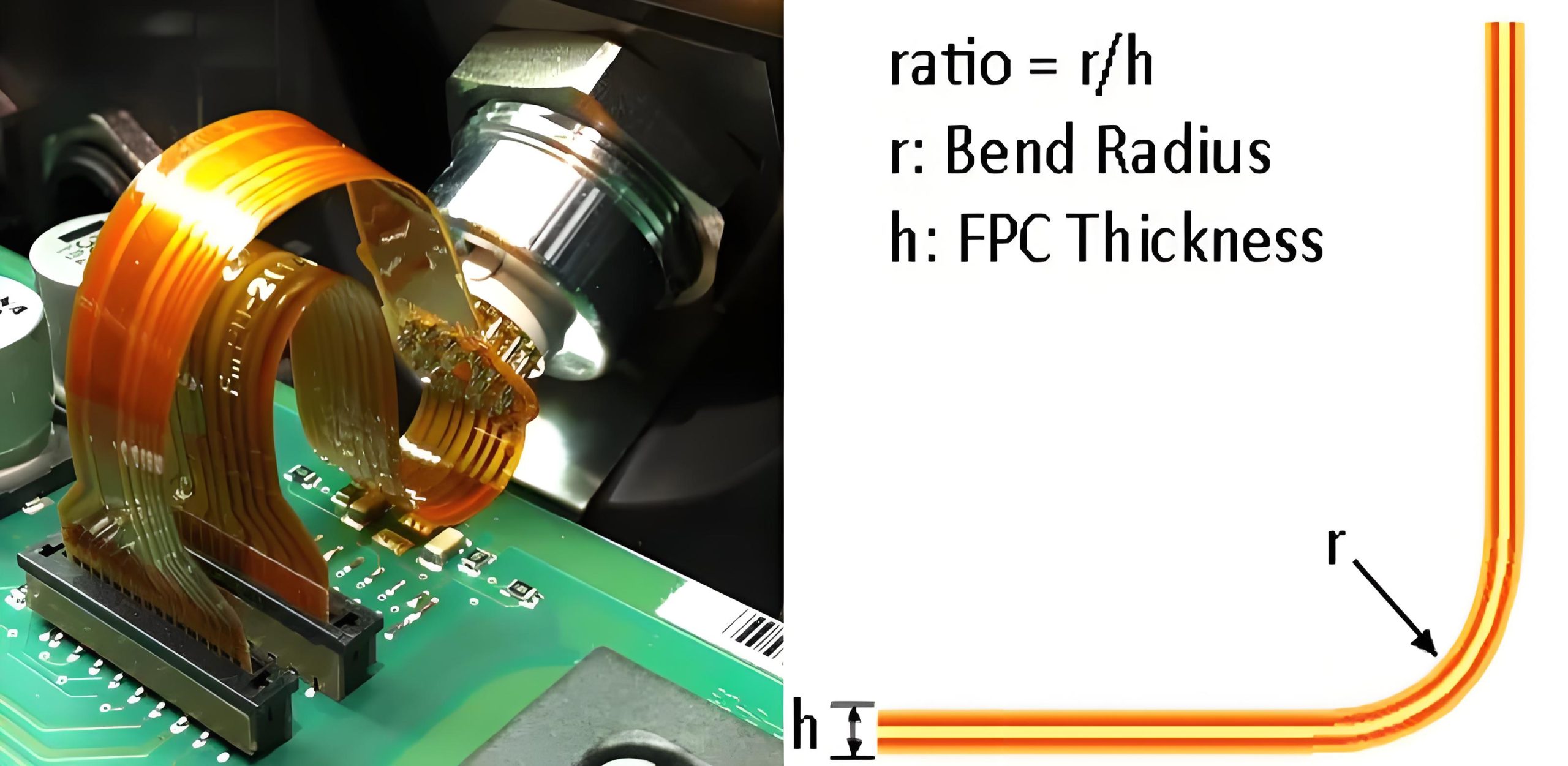
4.1 Bend Radius and Routing Rules
IPC-2223 specifications require strict control of bend radius in flexible areas. For a 2-layer flex structure (total thickness approximately 0.25mm), the recommended minimum bend radius for static flex (Bend-to-Install) is 2.5mm (약 10:1 ratio). For dynamic flex (>100,000 사이클), the minimum radius reaches 37.5mm (약 100:1 ratio). IPC reliability data indicates that 78% of flexible PCB failures originate from bend radius violations.
UGPCB strictly follows these principles during design:
-
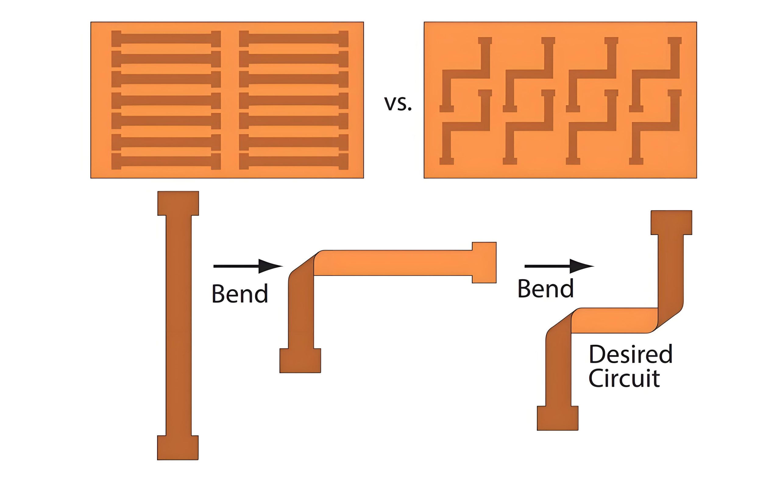
Routing Direction: All signal traces passing through the bend area must run perpendicular to the bend axis. Traces parallel to the bend axis experience maximum tensile stress during bending. Failure risk increases approximately 300%.
-
Via Avoidance: Do not place PTH vias and component pads within the bend area. The distance from via to bend start line must be at least 3× board thickness.
-
Copper Selection: Flexible layers use rolled annealed copper (RA Cu). RA copper offers elongation >15%, far superior to the electrodeposited copper (ED Cu) used in rigid layers. This allows RA copper to withstand repeated bending without fatigue fracture.
4.2 Layer Stackup Design
Stackup is the core determinant of rigid-flex PCB performance. This solution uses a 4-layer rigid plus 2-layer flexible asymmetric/symmetric structure. Rigid and flex layers bond with No-Flow PP. A balanced stackup design effectively controls warpage risk from CTE mismatch. UGPCB employs an Air-gap structure. The flexible area retains only the PI substrate. Rigid FR4 material is completely routed away from the flex area. This achieves maximum bending freedom.
4.3 임피던스 제어
임피던스 제어 is critical for MIPI CSI-2/C-PHY high-speed differential signals in camera modules. These signals typically exceed 2.5 Gbps per lane data rates. You can estimate characteristic impedance Z₀ using the IPC-2141A microstrip/stripline formula:
Stripline Impedance Approximation Formula:
z₀ = (87 / √(εᵣ + 1.41)) × LN(5.98시간 / (0.8w + 티))
Where H = dielectric thickness, w = 흔적 너비, t = 구리 두께, and εᵣ = dielectric constant.
UGPCB uses professional impedance calculation software such as Polar Si9000 for precise simulation during the design phase. We verify actual impedance using TDR (Time Domain Reflectometer) measurement. We ensure differential impedance stays within 100Ω ±10% tolerance. This meets MIPI Alliance specification requirements.
4.4 Rigid-to-Flex Transition Zone Design
The transition zone is the most vulnerable structural node in rigid-flex PCB design. IPC-2223E defines clear requirements for dielectric thickness, hole-to-edge spacing, and conductor layout in bend areas. UGPCB implements tapered trace transitions (avoiding sharp corners) and teardrop reinforcement in the transition zone. This design effectively reduces stress concentration at pad-trace junctions. Studies show stress reduction of approximately 40%.
4.5 Microvias and HDI Technology
This solution supports laser-drilled microvias for high-density routing demands in camera modules. Minimum hole diameter reaches 0.2mm. After laser drilling, O₂/CF₄ plasma cleaning (plasma desmear) removes carbonized residues from the PI surface. This process ensures strong copper plating adhesion within the hole wall.
5. Materials and Performance Specifications
5.1 Rigid Area Material: FR4
The rigid section uses 하이 -Tg (glass transition temperature) FR4 material. FR4 is the most widely used rigid substrate in global PCB manufacturing. It consists of epoxy resin impregnated fiberglass cloth. Standard FR4 Tg is approximately 130°C–140°C. High-Tg FR4 reaches Tg 170°C–180°C. This allows the board to withstand lead-free reflow soldering temperature windows without delamination or deformation.
5.2 Flexible Area Material: PI (폴리이미드)
The flexible section uses PI (폴리이미드) 기판. This is the core material for the flexible printed circuit industry. This solution uses adhesiveless PI, also known as 2L-FCCL (double-layer flexible copper clad laminate). Compared to traditional 3L-FCCL (adhesive-containing structure), adhesiveless PI offers significant advantages:
| Comparison | 2L-FCCL (Adhesiveless) | 3L-FCCL (Adhesive-Based) |
|---|---|---|
| Via Reliability | 높은 (no adhesive contamination in PTH) | 가난한 (adhesive affects hole wall bonding) |
| 최대 작동 온도 | 105–200°C | 85–160°C |
| 치수 안정성 | 높은 | 낮추다 |
| Flexural Endurance | 훌륭한 | 좋은 |
| 비용 | Slightly higher | 낮추다 |
Take DuPont™ Pyralux® AP all-polyimide double-sided copper clad laminate as an example. This material delivers the following key electrical performance:
-
유전 상수 (DK): 3.4 @ 1 MHz, 3.2 @ 10 GHz
-
소산 인자 (Df): 0.002 @ 1 MHz, 0.003 @ 10 GHz
-
유리전이온도 (Tg): 220℃
-
UL flammability rating: 94 다섯-0
-
UL maximum operating temperature (MOT): 200℃
-
Low outgassing characteristics: meets NASA space-grade standards
Pyralux® AP holds UL 94V-0 certification and complies with IPC 4204/11 사양. It is an ideal choice for manufacturing high-reliability multilayer flexible circuits and rigid-flex PCBs.
5.3 동박 종류
-
Flexible Layer Copper: Uses rolled annealed copper (RA Cu), 두께 1 온스 (약 35μm). RA copper grains elongate along the rolling direction. This provides excellent ductility and bending fatigue resistance. It is suitable for dynamic applications requiring repeated flexing.
-
Rigid Layer Copper: May use electrodeposited copper (ED Cu), also 1 OZ thickness.
6. Structural Parameters and Technical Specifications
This product uses a composite structure of 4 rigid layers (리지드 4L) plus 2 flexible layers (플렉스 2L). Technical specifications appear below:
| 매개 변수 | 사양 | Industry Comparison and Notes |
|---|---|---|
| 보드 유형 | 리지드 플렉스 PCB (유형 4) | Contains 6 total conductive layers; conforms to IPC-6013 Type 4 분류 |
| Rigid Material | FR4 (높은 Tg) | Tg > 170℃, suitable for lead-free reflow soldering |
| Flex Material | PI (폴리이미드, Adhesiveless) | Excellent heat resistance (MOT 200°C) and flex life |
| Rigid Layer Count | 4 레이어 | Meets medium-complexity signal routing and power plane requirements |
| Flex Layer Count | 2 레이어 | Supports differential signal transmission and return path design |
| 완성된 보드 두께 | 0.3mm | Suitable for space-constrained applications such as smartphone camera modules |
| 구리 두께 | 1 온스 (대략. 35μm) | Balances current-carrying capacity and trace precision |
| 표면 마감 | NiPdAu (Electroless Nickel/Palladium/Immersion Gold) | Excellent solderability and oxidation resistance; gold thickness 3μ” |
| 최소 구멍 크기 | 0.2mm (대략. 8밀) | Supports laser-drilled HDI technology |
| 최소 추적/공간 | 3밀 / 3밀 (대략. 0.076mm) | Meets high-density routing requirements |
| 기본 애플리케이션 | 카메라 모듈 PCB | 스마트폰, security surveillance, 자동차 카메라 모듈 |
Industry comparable rigid-flex PCB products typically range from 0.6mm to 3.2mm finished thickness. Common minimum drill diameter is 0.20–0.25mm. Minimum trace/space is approximately 0.05mm (2밀). UGPCB achieves 0.3mm finished thickness with 3mil fine traces and 0.2mm microvias. This demonstrates industry-leading process capability for camera module applications.
7. 표면 마감: NiPdAu (에네픽) 깊은 다이빙
This solution uses NiPdAu (Electroless Nickel/Palladium/Immersion Gold) as the final surface finish. This is a premium option among rigid-flex PCB surface finishes.
The NiPdAu structure deposits layers sequentially on the copper surface: nickel layer (대략. 3-6μm), palladium layer (대략. 0.05–0.15μm), and gold layer (대략. 0.05–0.1μm; this solution uses 3μ” ≈ 0.076μm gold thickness). The nickel layer acts as a diffusion barrier, preventing copper migration to the surface. The palladium layer is the key functional layer. It prevents nickel oxidation and provides excellent solderable surface for subsequent soldering. The extremely thin gold layer protects the palladium layer.
NiPdAu offers significant advantages over traditional ENIG (전기 니켈/침지 금). In ENIG processes, gold deposits directly on nickel. Excessive gold thickness or improper process control can cause “Black Pad” defects. This leads to brittle solder joint fractures. NiPdAu replaces some gold with palladium. This fundamentally eliminates black pad risk. NiPdAu also shows excellent compatibility with both aluminum wire bonding and gold wire bonding. This makes it particularly suitable for Chip-on-Board (CoB) packaging of CMOS image sensors in camera modules.
The IPC reference for this surface finish is IPC-4556, Specification for Electroless Nickel/Electroless Palladium/Immersion Gold (에네픽) Plating for 인쇄 회로 기판.
8. 제조 공정 흐름
Rigid-flex PCB manufacturing ranks among the most complex and tightly controlled processes in the PCB industry. Estimated process steps for rigid-flex circuitry are approximately three times those required for multilayer PCB manufacturing. The main production flow follows:
Stage One: Rigid Inner Layer Fabrication
-
재료 준비: Cut FR4 copper clad laminate to production size.
-
내부 레이어 이미징: Form circuit patterns on rigid inner layers using dry film exposure, 개발, and etching.
-
AOI 검사: Perform automated optical inspection for open/short defects in inner layer circuits.
Stage Two: Flexible Layer Fabrication
-
PI Material Prep: Cut adhesiveless PI copper clad laminate.
-
Flex Layer Imaging: Form circuit patterns on PI substrate (2 레이어).
-
Coverlay Lamination: Laminate PI coverlay film onto flexible circuit surface. Open pad windows using laser or die cutting.
-
혈장 청소: Remove residues from PI surface to improve interlayer adhesion.
Stage Three: Lamination and Rigid-Flex Integration
-
레이업: Stack rigid layers, No-Flow PP (low-flow prepreg), and flexible layers in sequence per design drawing.
-
진공 라미네이션: Press rigid and flexible materials into a single unit under high temperature and pressure.
-
Depth Routing: Use precision depth-controlled routing to remove rigid FR4 material from flexible areas. This exposes the flexible PI layer. This is the most critical step in rigid-flex PCB manufacturing. Depth accuracy must typically stay within ±0.05mm.
Stage Four: Subsequent Processing
-
교련: Perform mechanical through-hole drilling and laser microvia drilling.
-
Plasma Desmear: Remove carbonized residue and drill smear from hole walls.
-
PTH Electroplating: Deposit copper on hole walls to achieve interlayer electrical interconnection.
-
외부 레이어 이미징: Form outer layer circuit patterns.
-
Solder Mask Printing: Print solder mask ink on rigid areas.
-
표면 마감: Deposit NiPdAu plating.
-
Profile Routing: Cut final outline using laser or die punching.
-
Electrical Test and Final Inspection: Conduct flying probe test, 임피던스 테스트, 육안 검사, 그리고 AOI.
9. Product Features Summary
Based on the materials, 프로세스, and structural design described above, UGPCB Rigid 4L + Flex 2L solution offers these core advantages:
-
Ultra-Thin Profile: 0.3mm finished board thickness meets extreme space constraints of smartphones, 웨어러블, and other miniaturized applications.
-
Connector-Free Integrated Design: Rigid-flex integrated interconnection eliminates traditional board-to-board connectors. Reduces component count by approximately 30–50%. Also fundamentally eliminates reliability risks from connector loosening due to vibration or drop impact.
-
3mil Precision Routing: Meets stringent line width/spacing requirements for MIPI high-speed differential signals in camera modules. Supports data rates exceeding 2.5 Gbps per lane.
-
NiPdAu High-Reliability Surface Finish: Eliminates black pad defects. Compatible with both gold and aluminum wire bonding. Meets CMOS sensor CoB packaging requirements.
-
0.2mm Microvia Capability: Supports laser-drilled HDI technology for higher routing density.
-
High Thermal and Flexural Endurance: Adhesiveless PI substrate plus RA copper foil combination ensures structural stability through multiple SMT reflow cycles and long-term flexing.
-
Strict IPC Standards Compliance: Design and manufacturing follow IPC-2223, IPC-6013, and other international standards. Quality is verifiable and documented.
10. 일반적인 응용 프로그램
Rigid-flex PCB technology has achieved widespread adoption across multiple industries. Market research data shows consumer electronics as the largest end-use segment, accounting for over 40% of demand. Automotive electronics and aerospace follow.
10.1 Smartphone Camera Modules
This is the core target application for this solution. Within smartphone camera modules, flexible printed circuits are critical components determining image quality. Rigid-flex PCBs perform these core functions in camera modules:
-
Sensor Mounting Platform: Rigid areas provide flat, stable pad surfaces for mounting high-resolution CMOS image sensors and DSP image processing chips.
-
High-Speed Signal Transmission: Flexible areas transmit MIPI CSI-2/C-PHY differential signals (4K/8K video streams) from the sensor to the smartphone mainboard processor.
-
3D Space Adaptation: Flexible sections bend around batteries, 안테나, and other components. This maximizes utilization of extremely limited Z-height space within smartphones.
-
Connector Interface: Flexible ends typically feature gold fingers or ZIF connector interfaces for reliable connection to the mainboard.
10.2 Other Consumer Electronics
-
Foldable Phone Hinge Areas: Require extremely high reliability, withstanding over 200,000 fold cycles. Samsung shipped 12 million foldable phones in 2025. Chinese brands contributed an additional 8 million units. Global foldable device installed base now exceeds 35 million units.
-
AI Smart Glasses: 그만큼 2025 industry outlook from TPCA and ITRI identifies AI glasses as a new growth driver for flexible PCBs.
-
스마트워치, TWS Earbuds, VR/AR Headsets: Use rigid-flex PCB technology to distribute electronic functions across multiple zones within constrained volumes.
10.3 자동차 전자
The Automotive Flex-Rigid PCB market reached US$3.66 billion in 2025. It is projected to grow to US$3.94 billion in 2026, 와 함께 11.61% cagr. Major applications include:
-
ADAS automotive camera modules (forward-facing, surround-view, DMS driver monitoring)
-
EV BMS (배터리 관리 시스템) voltage sampling boards
-
LED headlight modules and in-vehicle infotainment systems
10.4 의료 전자 장치
-
Implantable medical devices (such as cardiac pacemakers): Require extremely high reliability and biocompatibility. Typically must meet Class 3 표준.
-
Endoscope camera modules and portable ultrasound probes for diagnostic equipment.
10.5 항공우주 및 국방
-
Satellite onboard electronics, UAV flight control systems, 및 군사 통신 장비. Require low outgassing (meeting NASA standards), wide-temperature-range operation (-55°C ~ +125°C), and high vibration resistance.
11. Market Trends and Growth Outlook
The Rigid-Flex PCB market is on a steady growth trajectory. Global market size reached US$2.462 billion in 2025. Forecasts project US$3.471 billion by 2032, 와 5.1% cagr. The North America flexible PCB market was valued at US$1.7 billion in 2025. It is expected to reach US$2.9 billion by 2030, at a 10.9% cagr.
Core drivers propelling market growth include:
-
Consumer Electronics Miniaturization and Foldable Form Factor Adoption: 스마트폰, foldable displays, AI glasses, and other devices continue to demand higher space utilization and flexible interconnection.
-
Rising Automotive Electronics Penetration: Each smart electric vehicle carries an average of 8–12 cameras (ADAS + surround-view + DMS). This directly drives demand for rigid-flex PCBs in automotive camera modules.
-
5G and Data Center Upgrades: Millimeter-wave Massive-MIMO antenna arrays and 800G Ethernet switches require low-loss flexible interconnect substrates in increasing volumes.
-
Medical Device Portability: Wearable health monitoring devices and remote diagnostic terminals are driving demand for medical-grade rigid-flex PCBs.
12. UGPCB를 선택하는 이유는 무엇입니까??
UGPCB brings years of expertise in PCB manufacturing and PCBA assembly. We have accumulated extensive engineering experience and manufacturing capabilities in high-reliability printed circuit boards and high-density interconnect printed boards. When you choose UGPCB for your rigid-flex PCB needs, you gain:
-
Full Turnkey Service: 에서 PCB 레이아웃 design review to rigid and flexible PCB manufacturing, SMT 어셈블리, and finished product functional testing, we deliver complete PCB assembly turnkey solutions.
-
엄격한 품질 관리: Manufacturing processes strictly adhere to IPC-A-600 (Acceptability of Printed Boards) and IPC-6013 specifications. Each production batch includes comprehensive inspection reports.
-
Rapid Response and Technical Support: Our professional engineering team provides DFM (제조 가능성을위한 설계) reviews. We help customers identify and resolve potential manufacturability issues during the design phase. This shortens time-to-market.
-
Competitive Cost Structure: Supported by a mature supply chain and lean production management, we deliver competitive pricing without compromising high quality.
Whether you are developing next-generation flagship smartphone cameras, ADAS automotive vision systems, or high-precision medical imaging equipment, UGPCB can customize the optimal rigid-flex PCB solution for your requirements.
13. Request a Quote and Start Your Project
Are you facing these challenges?
-
Internal device space is extremely limited. Traditional connector solutions no longer meet stacking requirements.
-
High-speed signals show instability. Impedance matching is difficult to control.
-
You need a reliable supplier capable of both rigid-flex PCB manufacturing and SMT assembly.
The UGPCB professional team is ready to assist. We provide full-process support from technical consultation and prototype fabrication to volume delivery.
📧 Send inquiries to: sales@ugpcb.com
🌐 Visit our website: www.ugpcb.com
📞 저희에게 연락하십시오: Get instant quote and technical consultation
👇 Click the button below. Submit your Rigid-Flex PCB design files now. Receive a fast quote within 24 시간!


