

A Measurable Leap, and a Line That Still Holds
Anthropic published a research note in November 2026. It reported that its model Claude Fable 5.2 raised its score on an internal benchmark called PCB Gym from 25% к 69% for placement and rerouting tasks. On the public BenchCAD 2.1 benchmark, the same model scored 83.5% — nearly double the prior Fable 5.1 result. More tellingly, three prototype devices were fabricated directly from Claude’s design files. Diode Computers built a USB-C speaker puck, a voice-assistant hub, and a handheld virtual pet without the usual back-and-forth engineering changes.
This news invites two tempting misreadings. One says AI will soon take over PCB design. The other dismisses it because “it is still just a prototype.” Both miss the useful signal. AI has made a measurable jump in geometric reasoning and manufacturing-constraint tracking. Yet that capability remains locked inside the prototype stage. Between a board that powers up and a PCBA that ships, several validation gates still stand. For teams evaluating AI-assisted PCB design, the practical question is not “replace or ignore.” It is: which layer of engineering has moved, and which standards still sit with the human engineer?

Where the Leap Actually Happens: Geometry, Not Electrical Judgement
Anthropic attributes the gain to geometry rather than to deeper circuit knowledge. Early models misplaced support components far from the IC, or flipped connector orientation. Fable 5.2 instead prioritises high-speed, high-current, and noise-sensitive nets first. On the voice-assistant hub, it routed USB and Ethernet differential pairs with intra-pair length matching and spacing. It also added tuning snakes so signals arrive together.
These are not new rules. IPC-2221 has long guided length matching and symmetry for high-speed routing. На практике, intra-pair length tolerance is often held around ±10 mil, and serpentine bump spacing is usually kept at no less than five times the trace width to avoid disturbing differential-mode behaviour. What changed is that the model now recognises which nets belong to this class and executes those rules with minimal prompting. It also deletes and reroutes when a region becomes visually untraceable, rather than pushing a 95%-complete board forward.
That rerouting behaviour mirrors an experienced engineer’s judgement: knowing when to restart instead of patching with more vias and layer hops. Another detail points the same way. Claude wrote its own grid-search router for the hub and cut single-long-trace routing to about one second. It also widened spacing after noticing an audio clock line running close to Ethernet. This is tool-use at a meta level, not merely layout craft.
DFM Is a Constraint You Pay Throughout Design, Not a Checkbox at the End
“Fabbed directly, zero back-and-forth” deserves attention because real PCB supply chains rarely work that way. Fabricators raise engineering queries on solder-mask openings, annular-ring margin, hole-to-copper distance, and panelisation. If the design file ignores manufacturing tolerance, the queries multiply. Anthropic recorded a concrete case. DFM flagged six thin solder-mask slivers on the hub, and Claude fixed them by widening the mask openings without moving any components.
The constraints involved can be quantified against industry standards. For solder-mask thickness over conductors, IPC-6012 Класс 2 generally requires ≥10 μm, while Class 3 typically tightens this to 15–20 μm; thinner mask directly erodes dielectric withstand and chemical resistance. Annular ring follows basic geometry:
IPC-6012 sets the Class 2 minimum at 50 мкм (о 2 мил) after drilling and plating. Сорт 3 keeps the 50 μm floor but allows zero breakout on any layer. A complete ring calculation also subtracts drill registration tolerance, typically ±50 to ±75 μm on mechanical drills, because the hole does not land perfectly centred. Electrical clearance comes from IPC-2221B Table 6-1. It specifies 0.1 мм (4 мил) for 0–30 V on uncoated external conductors, rising to 2.5 мм в 500 В. Altitude above 2,000 m applies a correction factor:
where h is altitude in metres. For current capacity, IPC-2152 replaced the older IPC-2221 charts. Для 1 oz external copper at a 10°C rise, а 10 mil trace carries roughly 1.0 А, while internal traces carry about 50–70% of that value.
Fable 5.2’s DFM behaviour shows a degree of constraint prioritisation. It fixed issues that mattered and ignored a deliberate ground tie that the tool misreported as an error. Yet that is not the same as understanding why a limit exists or making a trade-off when standards conflict. Passing DFM means the design is geometrically manufacturable. It does not mean the design has been validated.
What the Certificate Does Not Cover — and Why That Matters for PCBA
Anthropic states the boundary plainly. The three devices remain early prototypes. They have not undergone electrical validation, antenna tuning, thermal testing, or commercial certification. They are not designed for mass production. Claude did not connect to test equipment or production machines, and physical assembly and testing stayed with Diode engineers.
From a PCBA reliability standpoint, the gap between “it works on a desk” and “it can be shipped” breaks down into specific gates. IPC-A-610 is the current acceptability standard, и Revision J was published in March 2024. It defines Class 1, 2, и 3 criteria for solder wetting, component alignment, cleanliness, and coating. Сорт 3 targets aerospace, медицинский, and defence assemblies, with materially tighter requirements on materials, покрытие, and inspection results. A board that has run on a bench for several weeks does not automatically meet Class 3 requirements for hole-wall copper thickness, thermal-stress delamination, or solder-mask adhesion. UL 796 evaluates bare boards for laminate flame rating, conductor adhesion, dielectric withstand, and arc resistance. А UL 94 material flame rating is not the same as a board-level UL 796 listing. Thermal testing and antenna tuning remain wholly untouched at the prototype stage. The former determines whether long-term current and temperature margins hold. The latter determines whether the RF path still performs near a real enclosure and a human body.
Суммируя, Fable 5.2 demonstrates end-to-end prototype generation under geometric and manufacturing constraints. It does not demonstrate the engineering sign-off capability that a production release demands. Release decisions, certification pathways, and volume risk still belong to people who can interpret standards and own test data.
What This Means for the PCB and PCBA Supply Chain
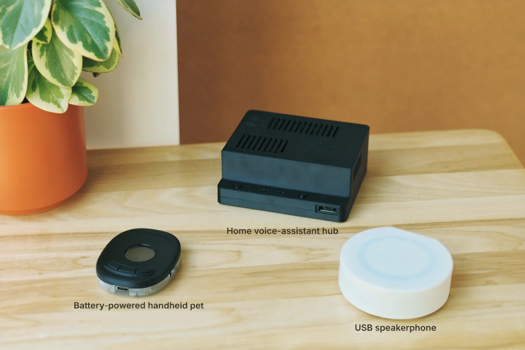
For teams seeking a PCB prototype quote or a quick-turn PCBA supplier, the practical value of this research is not “let AI release the board.” It is that friction between design files and manufacturing capability may fall. When an AI-generated design already pulls solder-mask openings, annular-ring margin, расстояние, and current-carrying widths into a fabricator-acceptable range during DFM self-check, the number of engineering-query rounds can drop. For fast-iteration prototypes, that can shorten the window from frozen specification to a powerable board. For low-volume PCBA projects that need a quote, a cleaner design package also helps suppliers return a firmer price and lead time.
Selection decisions still need engineering judgement. Before sending a prototype or PCBA inquiry to any supplier, confirm four things. Первый, electrical clearance should be calculated against the target market’s safety framework — IPC-2221B, МЭК 62368-1, or applicable UL 796 clauses — with altitude and coating corrections recorded. Второй, annular ring should carry registration margin under the intended IPC-6012 class. Third, solder-mask thickness and openings should sit inside IPC-6012 and IPC-A-600 acceptance ranges. Fourth — and most often skipped — the “zero-revision working” result at prototype stage should be explicitly labelled as preliminary functional confirmation without electrical validation or thermal testing, not as a production release basis.
AI has raised the quality of the first geometric and DFM draft. That genuinely lowers the cost of starting a prototype iteration. But PCB and PCBA professionalism was never only about routing a board that powers on. It is about knowing which certificate, which test, and which standard clause decide whether that board can be signed off. That line still belongs to the engineer.
Data Sources
- PCB Gym 69% против 25%, BenchCAD 2.1 83.5%, three zero-revision prototypes, and the prototype-stage limitations: Anthropic research note Testing Claude on real-world electronics design (9 ноябрь 2026).
- IPC-2221B Table 6-1 clearance values (0.1 mm at 0–30 V, 2.5 мм в 500 В) and the altitude correction factor: PCBSync and Atlas PCB summaries of IPC-2221B.
- Annular ring formula, IPC-6012 Класс 2 minimum of 50 мкм, and drill registration tolerance: Atlas PCB engineering guide.
- IPC-A-610 Revision J publication date (Маршировать 2024) и класс 3 criteria: Digi-Key and Escatec standard guides.
- IPC-2152 current capacity for 1 oz external copper at 10°C rise: Atlas PCB trace-width guide.
- UL 796 board-level evaluation versus UL 94 material flame rating: Atlas PCB UL certification notes.
