

В лаборатории тихо за полночь. Глазковая диаграмма на вашем осциллографе для этого 28 Сигнал Gbps PAM4 просто отказывается открываться — чрезмерный джиттер, рваные края — и вы проверили импеданс, соответствие длины, и стек. Все выглядит “стандарт.” Затем вы подметаете TDR (рефлектометр во временной области) вдоль следа жертвы и обнаружить, что форма сигнала шума соответствует фронту переключения тактовой линии, проходящей рядом с ним.. Это не воображение. Это перекрестные помехи — бесшумная передача энергии между двумя параллельными дорожками..
Емкостная связь и индуктивная связь: Два скрытых пути
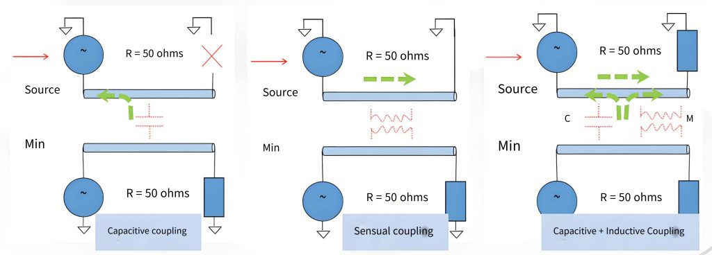
Перекрестные помехи возникают из-за электромагнитной связи между соседними межсоединениями., опосредовано двумя различными механизмами.
Емкостная связь передает энергию через паразитную емкость между дорожками. Чем быстрее меняется напряжение (дВ/дт) на линии агрессора, тем больший шумовой ток вводится в линию пострадавшего через взаимную емкостьСₘ. Индуктивная связь передает энергию посредством взаимной индуктивностиЛₘ — текущее изменение (ди/дт) на агрессора наводит на жертву шумовое напряжение.
Общее напряжение перекрестных помех может быть выражено в соответствии с рамками, установленными в IPC-2221., стандарт проектирования фундамента для печатных плат и других компонентов, монтирующих или соединяющих конструкций:
Vₙ = k × (В_д × С_д + Я_д × Л_д)
где *k* — коэффициент связи, C_d это распределенная емкость, иЛ_д это распределенная индуктивность.
Данные измерений рисуют четкую картину. Для 50 Ом микрополосковая линия с 8 ширина трассы в милах и 4 толщина диэлектрика в милах, увеличение расстояния от 8 мил (1Вт) к 12 мил (1.5Вт) уменьшает пик емкостных перекрестных помех примерно 35%. Дальнейшее увеличение до 16 мил (2Вт) дает лишь дополнительную 9% снижение. Это указывает на то, что за пределами 3 Вт (24 мил), предельная выгода резко уменьшается — амплитуда перекрестных помех не масштабируется линейно с расстоянием, а экспоненциально затухает..
Ближний конец против. Дальний конец: Разные направления, Разное поведение
Перекрестные помехи на ближнем конце (СЛЕДУЮЩИЙ) пары возвращаются к водителю в конце запуска сигнала агрессора. Его амплитуда может достигать 10% к 20% сигнала агрессора, но этоне зависит от длины муфты - как только длина связи превысит длину насыщения (примерно равно времени нарастания сигнала, умноженному на половину скорости распространения), СЛЕДУЮЩАЯ амплитуда перестает увеличиваться. NEXT зависит только от локальной геометрии.
Перекрестные помехи на дальнем конце (ФЭКТ) появляется на дальнем конце сигнала, и его амплитуда пропорциональна длине связи, но диэлектрические потери подавляют высокочастотные компоненты., поэтому более длинные следы иногда производятменьше ФЭКТ.
А 28 Моделирование канала PAM4 на Гбит/с наглядно это иллюстрирует.: в 15 мм длина муфты, максимум FEXT достигает -28 дБ. Распространение на 30 мм улучшает FEXT до -31 дБ из-за затухания высоких частот.
На твердой базовой плоскости, емкостной и индуктивный вклады в перекрестные помехи примерно равны по величине. Для ФЭКТ, они противоположны по полярности и имеют тенденцию к взаимному уничтожению — вот почемуполосковые структуры обладают более низким FEXT. Микрополосковые линии, однако, имеют электрические поля, частично проходящие через воздух, создание дисбаланса между емкостной и индуктивной связью, что делает FEXT значительным.
Правило 3W: Эффективный, но с предварительными условиями
The “3W Правило” практически инстинктивно для большинства печатная плата инженеры — сохраняйте расстояние между дорожками, как минимум в три раза превышающее ширину дорожки.. Но многие упускают из виду его предпосылки.
Когда межцентровое расстояние достигает 3 Вт., примерно 70% энергия электрического поля ограничивается внутри каждой диэлектрической области, снижение емкости связи до приемлемого уровня. Различные уровни промежутков дают следующие характеристики затухания перекрестных помех:
| Интервал трассировки | Затухание перекрестных помех | Оценка |
|---|---|---|
| 1Вт | Примерно -20 дБ | Значительный, неприемлемо |
| 2Вт | Примерно -30 дБ | Умеренный |
| 3Вт | Примерно -38 дБ | Приемлемо для большинства конструкций |
| 4Вт | Примерно -42 дБ | Отличный |
Правило 3W может удерживать перекрестные помехи ниже -35 дБ, что приемлемо для большинства конструкций. Однако, этот вывод опирается на три предварительных условия: непрерывная базовая плоскость, однородные диэлектрические свойства, и рабочие частоты ниже 5 ГГц.
Данные измерений на 50 Микрополосковая линия Ом показывает, что уменьшение расстояния с 3W до 2W ухудшает качество NEXT примерно 9 дБ. Если базовая плоскость имеет зазоры, деградация переходит в 15 дБ. Для дизайнов выше 28 Гбит / с (Частота Найквиста при 14 ГГц), рассмотрите расстояние от 5 до 7 Вт в сочетании с дополнительными методами подавления.
Следы охраны и контроль обратного пути: Более эффективно, чем использование одного интервала
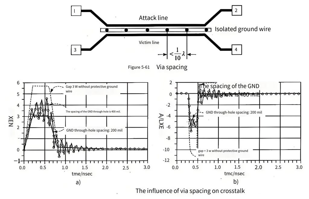
Размещение заземленных охранных следов по обе стороны от линии пострадавшего, с заземляющими отверстиями каждый 100 к 200 мил, может сократить NEXT более чем 20 дБ.
А 10 Пример использования объединительной платы Gbps демонстрирует эффективность: соседние пары LVDS без заземления через изоляцию выставлены 180 индуктивные перекрестные помехи mVpp. Добавление ряда 0.3 мм заземления каждые 10 мм уменьшил перекрестные помехи до 75 mVpp — снижение почти 60%.
Фигура 2: Защитная трассировка с заземлением через массив — сравнение подавления перекрестных помех
Основные соображения по проектированию трассировки защиты:
- Поддерживайте расстояние не менее 3 Вт между защитной и сигнальной дорожками, чтобы избежать дополнительной емкостной связи.
- Расстояние между переходами должно быть ≤ λ/10. (где λ — длина волны на самой высокой частоте сигнала.)
- Для 10 Сигналы Гбит/с, ограничить землю через расстояние между массивами не более чем 6 мм
Контроль обратного пути оказывается более эффективным, чем простое увеличение интервала. Уменьшение расстояния между сигналом и опорной плоскостью с 8 мил к 4 mil усиливает ограничение электрического поля и снижает коэффициент индуктивной связи примерно на 40%. Вот почемумаршрутизация сигналов вблизи сплошного заземления по своей сути подавляет перекрестные помехи.
Диагностика и стратегия: Сначала определите доминантный механизм
Первым шагом в подавлении перекрестных помех является не слепое увеличение интервалов или добавление защитных трасс.диагноз. Используйте TDR или VNA, чтобы проследить след жертвы и изучить взаимосвязь между формой связанного шума и сигналом агрессора.:
- Шумв фазе с агрессором →емкостная связь доминирует → отдать приоритет увеличению расстояния, изменение слоев, и сокращение параллельных прогонов
- Шумне в фазе с агрессором →доминантная индуктивная связь → уделить первоочередное внимание сокращению обратного пути, прокладка ближе к земле, и добавление охранных следов
Управление перекрестными помехами сводится к пониманию того, какая связь доминирует: емкостная или индуктивная., затем применяя правильное средство. Увеличение расстояния между адресами емкостной связи. Управление обратным путем решает индуктивную связь. Защитные дорожки и переходные отверстия обеспечивают комплексную защиту.. Ни один метод не работает для каждого сценария..
Декларация источника данных:
Ссылки на стандарты IPC в этой статье основаны на IPC-2221.Общий стандарт проектирования печатных плат. Данные по затуханию перекрестных помех по правилу 3W ссылаются на стандартные рекомендации по проектированию и проверку моделирования.. The 28 Данные моделирования канала PAM4 Гбит/с ссылаются на литературу по проектированию целостности высокоскоростного сигнала.. Описания механизмов связи NEXT и FEXT справочные источники учебников по целостности сигналов.
