
В компактных силовых модулях, блоки управления транспортными средствами на новых источниках энергии, или мощное промышленное оборудование, печатная плата дизайнеры часто сталкиваются с серьезной проблемой: как безопасно управлять высоким напряжением на ограниченном пространстве платы? Казалось бы, незначительная ошибка в расчете расстояния может привести к дуговому разряду., нарушение изоляции, или даже инциденты безопасности. В этой статье представлен углубленный анализ двух основных концепций высоковольтной разводки — зазор и путь утечки — и заложена надежная основа безопасности для вашей печатной платы и печатная плата дизайн, основанный на авторитетных стандартах.
Разъяснение концепции: Фундаментальная разница между зазором и утечкой
Первый, мы должны четко определить эти две концепции безопасности, которые часто путают.. В соответствии с МПК-2221Б (Общий стандарт на Дизайн печатной платы) и МЭК 60664-1 (Согласование изоляции оборудования в низковольтных системах):
-
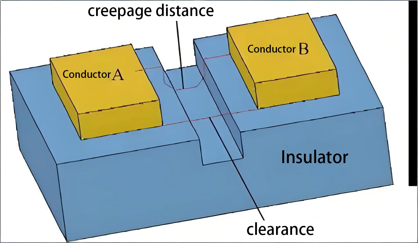
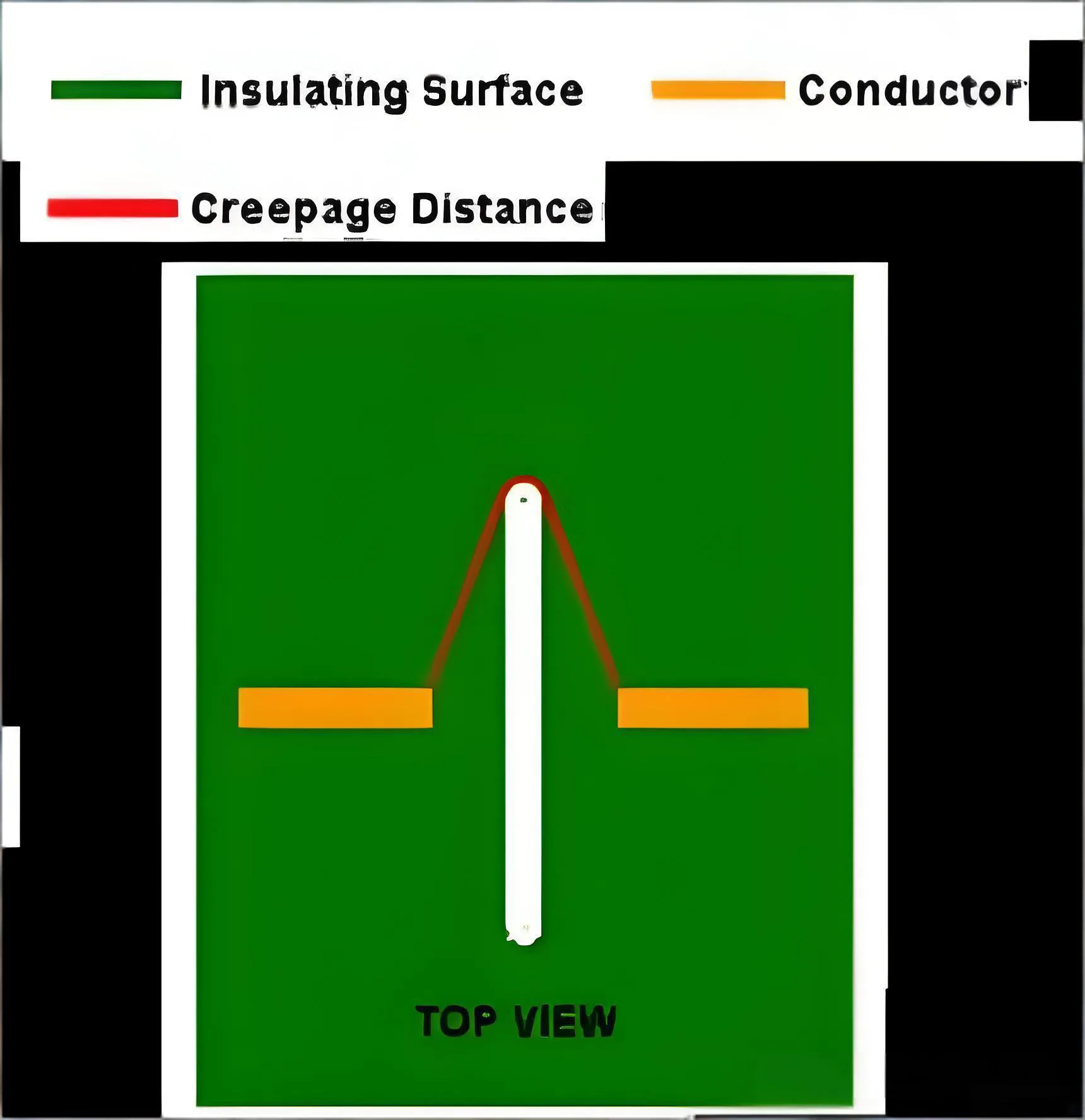
Распродажа: Кратчайшее прямолинейное расстояние в воздухе между двумя проводящими частями., или между проводящей частью и корпусом оборудования. Прежде всего, он предотвращает разрушение воздушного диэлектрика высоким напряжением., вызывая мгновенное искрение. Думайте об этом как о “расстояние по прямой, чтобы перелететь каньон.”
-
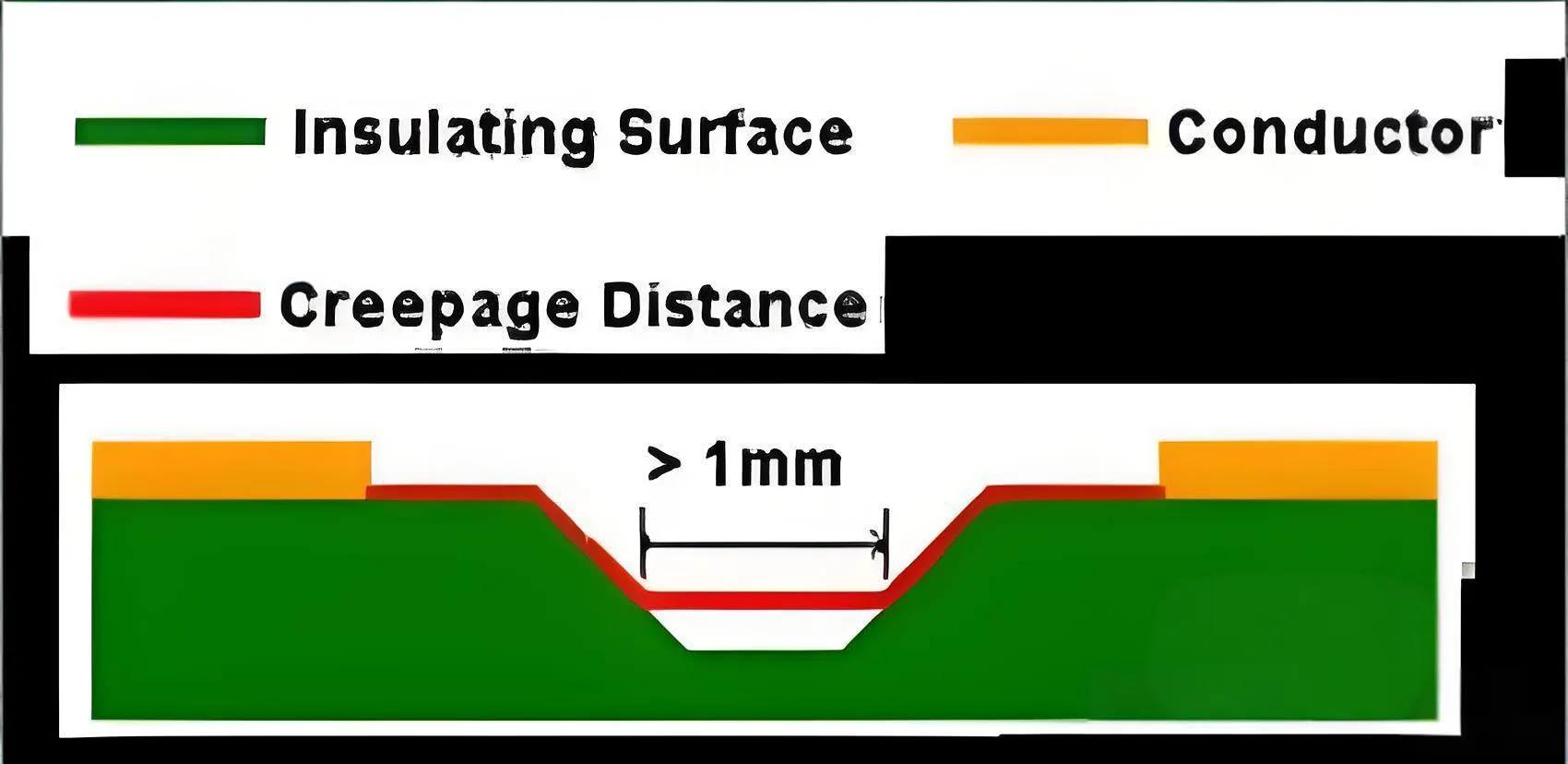
Расстояние утечки: Кратчайшая длина пути по поверхности изоляционного материала между двумя проводящими частями.. Прежде всего, это предотвращает попадание загрязнений. (например, пыль, влага, остаток флюса) от образования токопроводящего пути на поверхности изоляции, что приводит к медленной утечке или сбою отслеживания. Это сродни “кратчайший путь, по которому муравей может проползти по стене каньона.”
Основное различие заключается в среде: человек полагается на воздух, другое касается состояния изоляционной поверхности. В средах с более высокой степенью загрязнения, Требования к пути утечки часто более строгие, чем требования к зазору..
Краеугольный камень дизайна: Авторитетные стандарты и спецификации проектирования печатных плат на основе данных
Дизайн без стандартов слеп. Для высокого напряжения дизайн печатной платы, инженеры должны соблюдать соответствующие стандарты безопасности (например, UL, МЭК, ГБ) в зависимости от области применения продукта (например, бытовая электроника, промышленный контроль, медицинское оборудование, автомобильная электроника). Среди них, МЭК 60664-1 является основополагающим международным стандартом, который обеспечивает метод проектирования справочной таблицы на основе рабочего напряжения., степень загрязнения, группа материалов, и категория перенапряжения.
Возьмем типичный импульсный источник питания переменного и постоянного тока. (вход 100–240 В переменного тока, со схемой PFC) защитная изоляция между первичной и вторичной сторонами в качестве примера, его требования к изоляции обычно включают:
-
Базовая изоляция: Фундаментальная защита от поражения электрическим током..
-
Усиленная изоляция: Эквивалент двойной основной изоляции., обеспечивающая более высокую надежность.
В соответствии с МЭК 62368-1 (Стандарт безопасности для аудио/видео, Оборудование информационных и коммуникационных технологий) и общие требования к сертификации, под Степень загрязнения 2 (общая промышленная среда), на рабочее напряжение 240ВАК (соответствующее пиковое напряжение ~340В), Требования к минимальным путям утечки и зазорам обычно следующие::
| Тип изоляции | Распродажа (Мин.) | Расстояние утечки (Мин., Группа материалов IIIa) |
|---|---|---|
| Базовая изоляция | 2.0 мм | 3.2 мм |
| Усиленная изоляция | 4.0 мм | 6.4 мм |
(Примечание: Вышеуказанные значения являются типичными.. Фактический проект должен полностью соответствовать процессу справочной таблицы выбранного стандарта., с учетом таких факторов, как высота над уровнем моря и переходное перенапряжение.)
Решения для ограниченной недвижимости на печатных платах: Пять инженерных стратегий
Когда пространство на плате ограничено и требования к расстоянию по прямой не могут быть соблюдены., опытный дизайн печатной платы инженеры используют следующие стратегии для эффективного увеличения длины пути утечки:
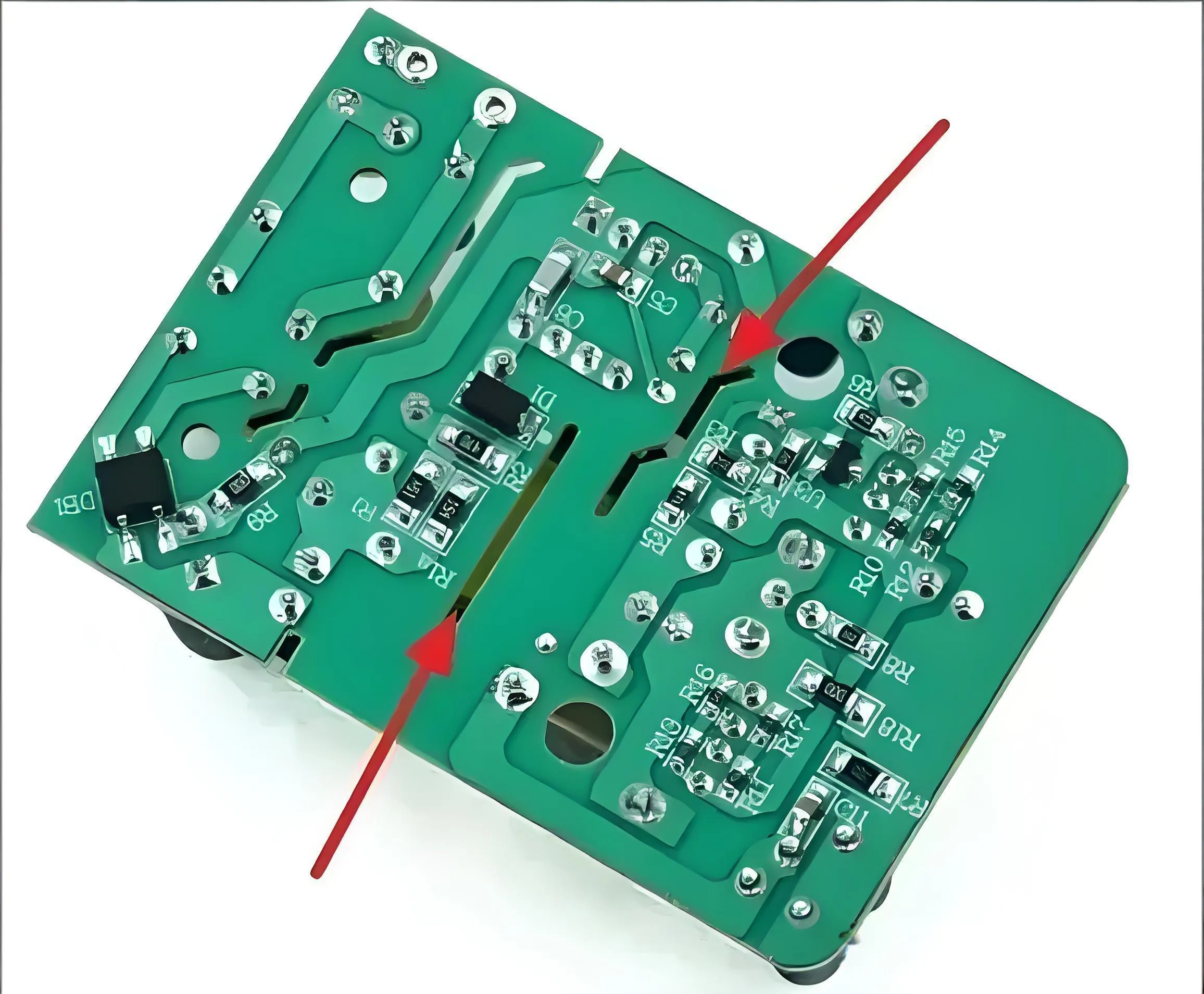
1. Прорезь для увеличения расстояния
Это самый классический и эффективный инженерный метод.. Отфрезеруйте или пробейте изоляционную прорезь в зоне заливки меди между двумя высоковольтными проводниками..
-
V-образный паз / U-образный паз: Подходит для умеренной компенсации расстояния. Слот не проникает в печатную плату; глубина обычно 1/3 к 2/3 толщины доски. Это эффективно заставляет путь утечки идти в обход стенки паза., значительно увеличивая расстояние до поверхности.
-
Длинный сквозной слот: Самый эффективный. Полностью проникающий изоляционный слот (часто ширина ≥1,0 мм) создается непосредственно между проводниками. Путь утечки должен проходить по всей длине паза., увеличение расстояния более чем в два раза по ширине прорези. Это распространенный метод изоляции первичной обмотки от вторичной в печатных платах импульсных блоков питания..
2. Обновление материала печатной платы
-
Выберите Высокопроизводительный Подложка PCB: Сравнительный индекс отслеживания (CTI) стандартного FR-4 обычно находится в диапазоне 175–250 В.. Выбор материалов с высоким CTI (например, специальные безопасные изоляционные материалы с CTI ≥600 В) позволяет сократить требования к пути утечки в соответствии со стандартами IEC. Например, Группа материалов I (КТИ ≥600 В) может потребоваться почти половина пути утечки группы IIIa (100V ≤ CTI <175В).
-
Используйте керамические подложки: Для конструкций со сверхвысокой плотностью мощности, такие как модули драйверов IGBT в автомобильных печатных платах., напрямую использовать оксид алюминия (Al₂O₃) или нитрид алюминия (Альтернативный) керамические субстраты. Керамика не только имеет чрезвычайно высокий CTI, но и отличную теплопроводность., фундаментальное устранение рисков слежения за поверхностью.
3. Улучшение покрытия поверхности печатной платы
Нанесите защитное покрытие или специальную антитрекинговую краску на участки печатной платы, находящиеся под высоким напряжением.. Это может улучшить сопротивление изоляции поверхности и в некоторой степени противостоять влаге и загрязнению.. Однако, Обратите внимание, что большинство стандартов безопасности (например, UL) не позволяют в полной мере полагаться исключительно на покрытия для уменьшения пути утечки. Это скорее вспомогательный метод армирования., качество покрытия и долговременная надежность должны быть подтверждены..
4. Трехмерное дизайнерское мышление
Думайте не только о 2D-планировании; использовать третье измерение.
-
Используйте изоляционные стены/барьеры: Припаиваем изолирующие пластиковые перегородки к печатной плате..
-
Используйте перемычки или вертикально установленные изоляторы.: Обеспечьте высоковольтные соединения с помощью пролетных проводов. (удовлетворительное разрешение), полностью избежать проблем с утечкой по поверхности.
5. Ключевые моменты процесса трансформатора
В изолированном исполнении импульсного источника питания, внутренняя изоляция трансформатора имеет решающее значение. Провод с тройной изоляцией или достаточные стенки катушки (плавает) должен использоваться между первичной и вторичной обмотками. Расстояние изоляции равно сумме ширин стенок с обеих сторон плюс воздушный зазор по длине намотки.. Штыри должны быть снабжены изоляционной трубкой., и трубка должна проходить через стенку шпульки, чтобы предотвратить “ярлык” поломка на штырях.
Проверка проекта и будущие тенденции
По завершении проектирования, строгая проверка с использованием DFM (Дизайн для производства) и ДФА (Проектирование для сборки) правила очень важны, специально для высоковольтных участков. Профессиональный Производители печатной платы и поставщики печатных плат должны обладать соответствующими возможностями проверки стандартов безопасности..
Заглядывая в будущее, по мере увеличения напряжения устройства и уменьшения размеров, распространение широкозонных полупроводников, таких как Карбид кремния (Карбид кремния) и ГаН (Нитрид галлия) создает более строгие проблемы для выдерживаемого напряжения печатной платы и теплового проектирования. Использование программного обеспечения для моделирования для предварительного анализа распределения электрического поля станет стандартным процессом проектирования высокопроизводительных силовых печатных плат..
Заключение
Проектирование безопасности высоковольтной разводки является концентрированным отражением профессионализма и чувства ответственности инженера по печатным платам.. Зазор и путь утечки — эти два невидимых элемента “красные линии безопасности” — обеспечивать долгосрочную надежность продукции и, что еще более важно, безопасность конечных пользователей’ жизни и имущество. В сегодняшнем стремлении к плотности мощности и эффективности, Освоение этих принципов безопасности и гибкое применение инженерных решений является важнейшим техническим препятствием, которое должен преодолеть каждый специалист, занимающийся проектированием высоковольтных печатных плат и производством высококачественных печатных плат.. Когда вы сталкиваетесь с такими проблемами проектирования, профессиональный консультант Поставщики печатной платы или поставщики услуг PCBA с богатым опытом в области стандартов безопасности, такие как УГКПБ, сотрудничество на ранних стадиях проектирования, несомненно, является лучшим способом снижения рисков и оптимизации затрат..

здесь столько замечательной информации, : Дюймовый.
Обычно я веду блог и восхищаюсь вашим контентом.. Статья действительно вызвала у меня интерес. Я добавлю ваш сайт в закладки и буду продолжать проверять новую информацию о брендах..