
Введение
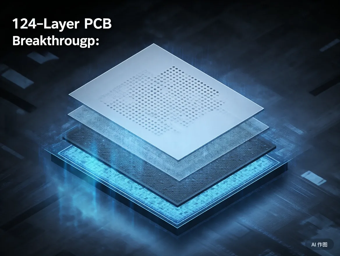
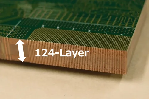
Движимый искусственным интеллектом (Ай) и высокопроизводительные вычисления (HPC), Глобальная электроническая индустрия проходит технологическую революцию, сосредоточенную на “высокая плотность, высокоскоростной, и высокая надежность.” В мае 2025, Ведущий Производитель печатных плат раскрыл первую в мире коммерческую 124-слойную печатную плату, Разрыв давний 108-слойный отраслевой барьер при сохранении стандартной толщины доски 7,6 мм. Эта веха не только обеспечивает критическую аппаратную поддержку для серверов искусственного интеллекта, полупроводниковое тестирование, и системы защиты, но также открывают новые границы в технологии электронной упаковки.
Разрушение 108-слойного барьера: Инженерные решения, стоящие за 124-слойными платы
Точные производственные инновации
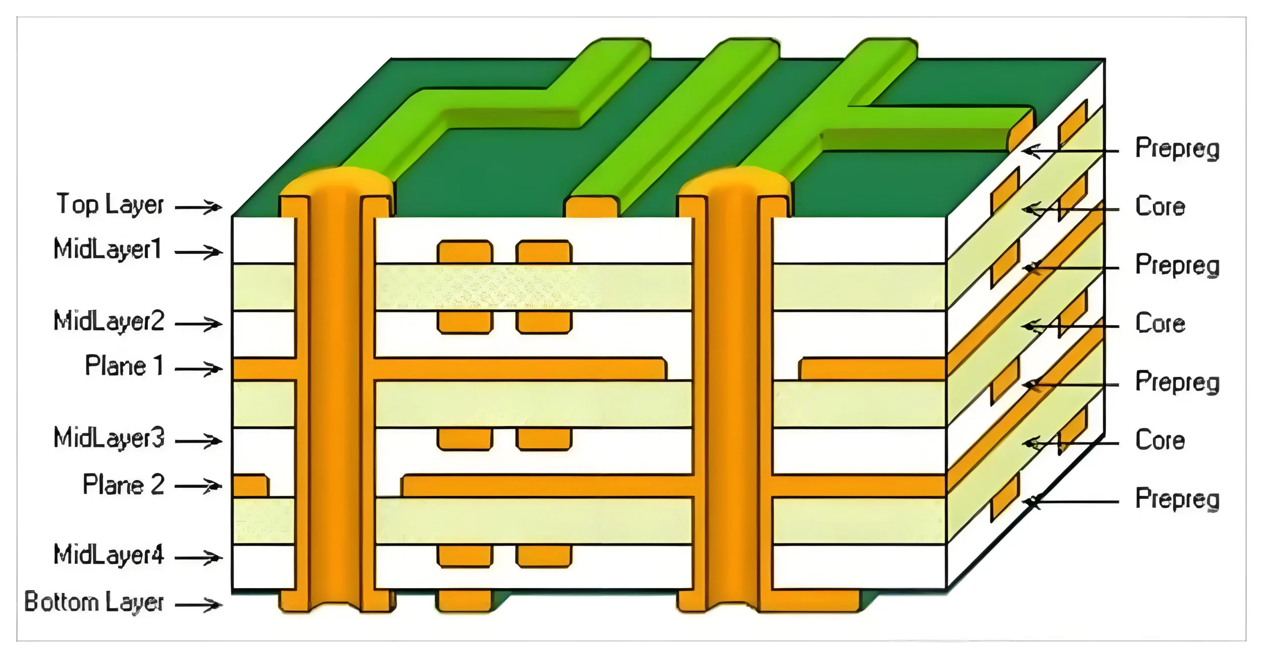
Традиционный Проекты печатных плат лицо механическим и термическим ограничениям в 100 слои из -за несоответствий потока смолы, через коллапс, и слоя смещения. Прорывная 124-слойная печатная плата достигает 15% Увеличение слоя до:
-
Ультратонкие диэлектрики: 25мкм слои с использованием материалов с низким содержанием потери (например, Упал 7) с контролем импеданса ± 5% для 112+ ГГц сигналы
-
3D Взаимосвязанная оптимизация: Массивы Microvia, обеспечивающие плотность сигнала 0,15 мм²/мм, Соответствие PCIE Gen6 и CXL 3.0 протоколы
Сертификация тепловой надежности
Сертифицировано в соответствии с стандартами MIL-STD-883G, 124-слойная печатная плата выдерживается 1,000+ термические циклы (-55° C до 125 ° C.) во время поддержания <1% Потеря сигнала в 80 MPA Механическое напряжение - делает его идеальным для аэрокосмических и оборонных применений.
Приложения: Ускорение аппаратных и полупроводниковых достижений
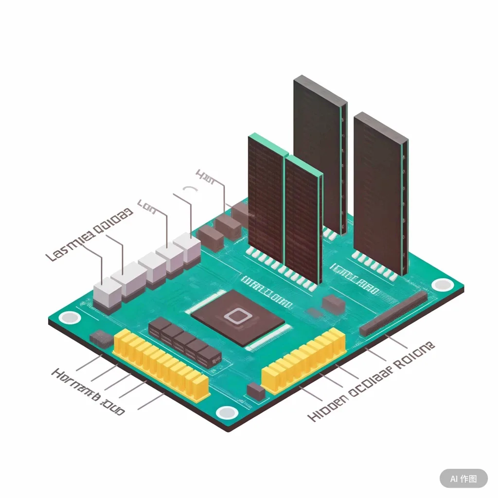
Серверы ИИ & Память с высокой пропускной способностью (HBM)
-
Плотность сигнала: 18% Увеличение дифференциальной пары маршрутизации на слое
-
Тепловое управление: Наполненная медью микроворией улучшает теплопроводность 30%, критическая для ускорителей 500 Вт+ ИИ
Тестирование на уровне пластины & 3D Упаковка
Обеспечивает точность выравнивания субмикронов (± 0,8 мм) и управление задержкой сигнала на уровне пикосекунда для уклаженных модулей HBM-изменение игры для архитектур на основе чиплета.
Проблемы стоимости & Масштабируемость дорожная карта
Производственная экономика
-
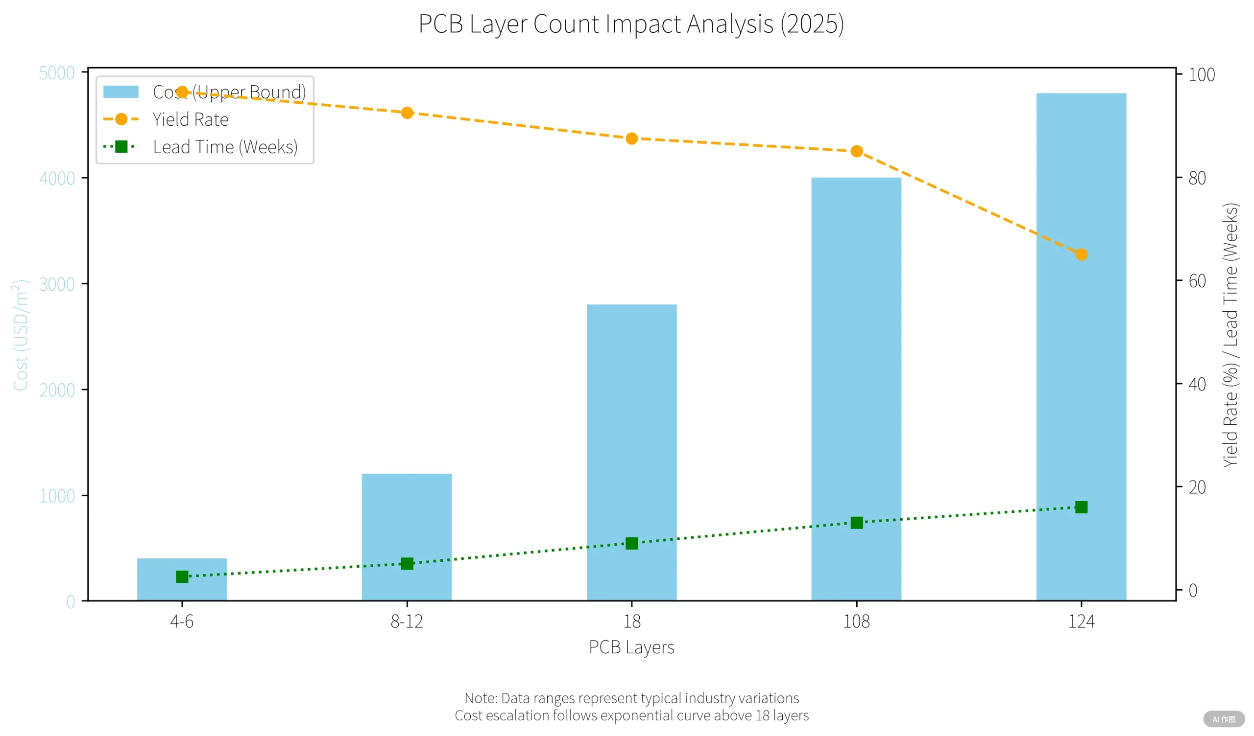
Стоимость материала: 4,800/М2(против.3,200/м² для 108-слойного)
-
Показатели доходности: 65% (16-недельный цикл) против. 85% для обычного ИЧР
-
Анализ неудачи: Разрушительное перекрестное сечение, необходимое для 20% дефектов теплового напряжения
Промышленные пути усыновления
-
Аддитивное производство: Уменьшает шаги ламинирования 40%
-
AI-управляемый Eda: Прогнозируется через точки стресса с 92% точность, потенциально повышает урожайность 75%
Перспективы рынка: $49B ПХБ отрасли трансформация
Драйверы роста
-
Облачные вычисления: 70% CAGR в печатных платах Server Server (Citic Securities 2026 проекция)
-
Устройства Edge AI: 30% Увеличение стоимости печатной платы на смартфонах следующего поколения (Данные цепочки поставок Apple)
-
Тенденции локализации: Китайским производителям нравится УГКПБ Органирование 3,6 м м²/год для продвинутых субстратов
Заключение: Практические инновации в отношении записей подсчета слоев
Не превзойдя 129-слойный прототип Денсо (2012), Эта 124-слояная печатная плата устанавливает новый коммерческий эталон через:
-
Стандартизированная толщина (7.6мм) Для обратной совместимости
-
Mil-Spec надежность в 85% прототип затрат
-
Масштабируемые производственные процессы
В качестве квантовых вычислений и 6G появляются, Инновация PCB будет определять приоритеты функциональной плотности по количеству слоев - критический сдвиг для устойчивого технологического прогресса.
